An automatic tinning device for pcb circuit boards

A technology for PCB circuit boards and tinning devices, which is applied in the direction of assembling printed circuits with electrical components, to achieve the effects of improving efficiency, facilitating vertical lifting, and easy transportation

Active Publication Date: 2022-07-19
启东新亚电子科技有限公司
View PDF3 Cites 0 Cited by
  • Summary
  • Abstract
  • Description
  • Claims
  • Application Information

AI Technical Summary

Problems solved by technology

[0005] The purpose of the present invention is to provide an automatic tinning device for PCB circuit boards to solve the problem of lack of necessary technical measures in the prior art to make the printed circuit boards be loaded into the fixture at a suitable angle and then transformed into a vertically suspended state. technical problem

Method used


Image

  • An automatic tinning device for pcb circuit boards
  • An automatic tinning device for pcb circuit boards
  • An automatic tinning device for pcb circuit boards

Examples


Embodiment Construction

[0037] The technical solutions in the embodiments of the present invention will be clearly and completely described below with reference to the accompanying drawings in the embodiments of the present invention. Obviously, the described embodiments are only a part of the embodiments of the present invention, but not all of the embodiments. Based on the embodiments of the present invention, all other embodiments obtained by those of ordinary skill in the art without creative efforts shall fall within the protection scope of the present invention.

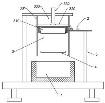
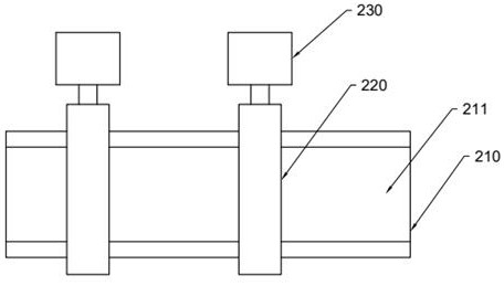
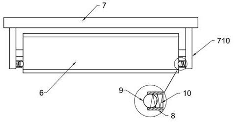
[0038] like Figure 1 to Figure 5 As shown, the present invention provides an automatic tinning device for a PCB circuit board, which is characterized in that it has:

[0039] Tin melting furnace 1, used to carry solder;

[0040] Feeding mechanism 2, used to transport PCB circuit boards horizontally;

[0041]The soaking mechanism 3 is arranged between the opening side of the tin melting furnace 1 and the feeding mechanism 2, and the...


PUM


Abstract

The invention discloses an automatic tinning device for a PCB circuit board, comprising: a tin melting furnace, a feeding mechanism, a dipping mechanism and a hot air leveling mechanism; wherein the dipping mechanism includes a material transfer clamping component and a reciprocating driving component, which rotates The assembly can regulate the rotation of the transfer and clamping assembly, so that the transfer and clamping assembly can receive the PCB circuit board of the feeding mechanism when it is in a horizontal state, and can be driven by the reciprocating driving assembly to descend into the tin melting furnace in a vertical state. In the present invention, the PCB circuit board is transported horizontally by the feeding mechanism, and the PCB circuit board is placed in a horizontal direction for easier transportation, and the manual feeding is replaced by a mechanical automation device, which greatly improves the feeding efficiency; The horizontal posture is transformed into a vertical hanging posture, which is convenient for the vertical lifting and lowering of the PCB circuit board to complete the tinning process.

Description

technical field [0001] The invention relates to the technical field of printed circuit board production, in particular to an automatic tinning device for PCB circuit boards. Background technique [0002] PCB (Printed Circuit Board) circuit board, the Chinese name is printed circuit board, also known as printed circuit board, is an important electronic component, a support body for electronic components, and a carrier for electrical interconnection of electronic components. [0003] In the production of printed circuit boards, tinning the surface of the printed circuit board and hot air leveling are essential processes. The specific operation process is: first apply flux on the printed circuit board, and then Hang the printed circuit board coated with flux on the fixture manually, and then move down through the lifting device, put the printed circuit board into the tin melting furnace, and make the printed circuit board in the tin melting furnace. Tin plating; after the prin...

Claims


Application Information

Patent Timeline
IPC IPC(8): H05K3/34
CPCH05K3/34
Inventor 杨新
Owner 启东新亚电子科技有限公司
Why Eureka
Try Eureka