Visible-infrared dual-band photoelectric detector

A photodetector and dual-band technology, applied in the direction of circuits, electrical components, semiconductor devices, etc., can solve the problems of detection spectral range limitation, limit application, restrict the development of silicon-based photodetectors, etc., achieve good transmission performance, broaden the Application fields, improving the effect of detecting the spectral range

Pending Publication Date: 2022-06-24
CHANGCHUN INST OF OPTICS FINE MECHANICS & PHYSICS CHINESE ACAD OF SCI
View PDF0 Cites 0 Cited by
  • Summary
  • Abstract
  • Description
  • Claims
  • Application Information

AI Technical Summary

Problems solved by technology

Since the bandgap width of silicon is about 1.1eV, silicon has a response in the visible light and near-infrared bands, but for photons with energy less than 1.1eV, due to the relatively large bandgap width of silicon materials, silicon photodetectors are in the middle and far infrared bands. The light absorption of silicon-based photodetectors is almost zero, which to a certain extent restricts the development of silicon-based photodetectors in the near-infrared and mid-to-far infrared light bands with wavelengths greater than 1.1 μm, and the existing silicon-based photodetectors mainly perform single-band spectral detection. , the detection spectral range is limited, and it has limitations in wide-band detection, which limits its application in some fields

Method used


Image

  • Visible-infrared dual-band photoelectric detector
  • Visible-infrared dual-band photoelectric detector
  • Visible-infrared dual-band photoelectric detector

Examples


Embodiment Construction

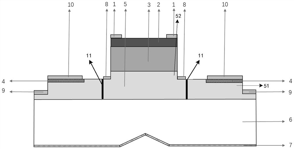
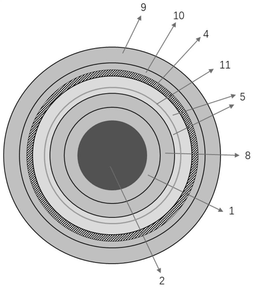
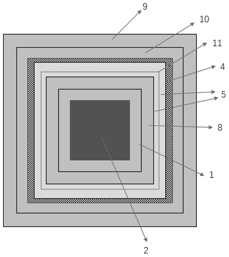
[0038] In order to enable those skilled in the art to better understand the solutions of the present invention, the following will clearly and completely describe the technical solutions in the embodiments of the present invention in conjunction with the drawings in the embodiments of the present invention. Obviously, the described embodiments are only It is an embodiment of a part of the present invention, but not all embodiments. Based on the embodiments of the present invention, all other embodiments obtained by persons of ordinary skill in the art without making creative efforts shall fall within the protection scope of the present invention.

[0039] The terms "first", "second", "third", "fourth" and the like in the description and claims of the present invention and the above drawings are used to distinguish similar objects, but not necessarily to describe specific sequence or sequence. It is to be understood that the terms so used are interchangeable under appropriate ...


PUM


Abstract

According to the visible-infrared dual-band photoelectric detector provided by the embodiment of the invention, the PIN photoelectric detection structure and the metal-semiconductor contact interface barrier structure are utilized, so that the quantum efficiency of middle and far infrared bands is improved, and meanwhile, the visible-infrared dual-band detection function of the photoelectric detector is realized. The detector has the advantages that when light is vertically incident, visible light is fully absorbed and detected by the PIN structure when passing through the PIN structure, and as silicon has good transmission performance for light in an infrared band, the light in the infrared band passes through the substrate layer and is reflected by the metal film reflecting layer, the light in the infrared band is reflected to the microstructure layer, and the light in the infrared band is reflected by the PIN structure. The characteristic of the microstructure layer is utilized to enhance absorption of infrared band light, so that a carrier obtains energy to jump to a Fermi level and cross a potential barrier to enter a semiconductor substrate, electrons and holes are collected by metal electrodes on the two sides respectively, high-quantum-conversion-efficiency absorption detection is performed on the infrared band light, visible-infrared dual-band detection is realized, and the visible-infrared dual-band detection is realized. According to the invention, the detection spectrum range can be greatly improved, and the application field is widened.

Description

technical field [0001] The invention relates to the field of optoelectronic technology, in particular to a visible-infrared dual-band photodetector. Background technique [0002] Silicon-based photodetectors, as the main force of detection devices in the visible and near-infrared bands, have the advantages of high efficiency, low power consumption, small size, anti-vibration, low price and easy integration with circuits, etc., and are widely used in various fields. Since the bandgap width of silicon is about 1.1eV, silicon has a response in the visible light and near-infrared bands, but for photons with energy less than 1.1eV, due to the relatively large bandgap width of silicon materials, silicon photodetectors are in the middle and far infrared bands. The light absorption of silicon-based photodetectors is almost zero, which to a certain extent restricts the development of silicon-based photodetectors in the near-infrared and mid-to-far infrared light bands with wavelength...

Claims


Application Information

Patent Timeline
Patent Type & Authority Applications(China)
IPC IPC(8): H01L31/109H01L31/0216H01L31/0236H01L31/0352
CPCH01L31/035209H01L31/02161H01L31/02363H01L31/109
Inventor 梁静秋李香兰王惟彪陶金吕金光秦余欣陈伟帅郭广通
Owner CHANGCHUN INST OF OPTICS FINE MECHANICS & PHYSICS CHINESE ACAD OF SCI
Why Eureka
Try Eureka