Method for improving infrared response of silicon-based detector through helium ion implantation

An infrared response, helium ion technology, used in semiconductor devices, sustainable manufacturing/processing, electrical components, etc., can solve the problems of inability to detect infrared band optical signals, weak response in infrared band, etc., to improve the detection spectral range and broaden the detection range. spectral range, the effect of improving the infrared response

Pending Publication Date: 2021-12-07
TIANJIN UNIV
View PDF0 Cites 1 Cited by
  • Summary
  • Abstract
  • Description
  • Claims
  • Application Information

AI Technical Summary

Problems solved by technology

Due to the limitation of the response mechanism, traditional silicon-based photodetectors ca

Method used


Image

  • Method for improving infrared response of silicon-based detector through helium ion implantation
  • Method for improving infrared response of silicon-based detector through helium ion implantation
  • Method for improving infrared response of silicon-based detector through helium ion implantation

Examples


Embodiment approach 1

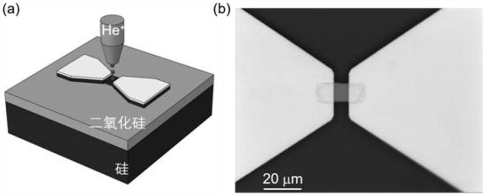
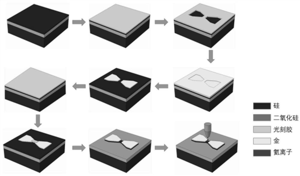
[0039] See figure 2 , Using a helium ion microscope helium ion implantation of silicon, silicon-based photoelectric when the optical power incident on the detector is changed, and the effects of surface defect states absorption state absorbing effect simultaneous action of the device will cause the photosensitive region admittance change. Silicon photodetector for monitoring the optical power of the infrared band can be achieved based on this phenomenon.

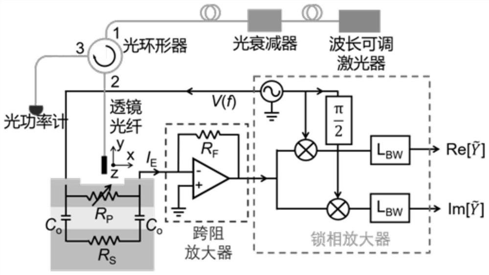
[0040] image 3 Schematic experiment optical power monitoring photodetector is a silicon implanted helium ions. Return to the lock signal outputted through the transimpedance amplifier (TIA) after amplification; lock-in amplifier outputs a variable frequency sinusoidal voltage, voltage from one end of the titanium electrode as the drive signal input device, and then output through the other end of the titanium electrode phase amplifier demodulates the converted admittance worth demodulation device.

Embodiment approach 2

[0042] After the helium ion implantation of the silicon photodetector to recalibrate: relationship obtained by the test device and the driving voltage source admittance operating frequency different light power, to find the most obvious change in the admittance as a working frequency point; determine the operating frequency again after the relationship between the optical power calibration admittance change at different wavelengths.

[0043] Figure 4The relationship between the silicon-based photodetector is introduced and the drive frequency of the silicon-based photodetector. Preliminary screening can be performed based on the features of these curves to confirm the appropriate helium ion implantation dose.

[0044] Figure 5 Inject 0.01ionS / Nm for helium ion 2 The silicon-based photodetector reflected optical power and the two-dimensional scaver map of the admission. With this figure, you can compare the location and contour of the device electrode and the photosensitive reg...


PUM


Abstract

The invention discloses a method for improving the infrared response of a silicon-based detector through helium ion implantation. The method comprises the following steps: injecting helium ions into a silicon material to generate a defect state, and when the power of light incident on the silicon-based photoelectric detector is changed, the defect state absorption effect and the surface state absorption effect act at the same time, so that the admittance of the photosensitive area of the silicon-based photoelectric detector is changed, and the silicon-based photoelectric detector can monitor the infrared band optical power. The silicon-based photoelectric detector is a vertical coupling transparent photoelectric detector based on a surface state absorption principle and comprises a photosensitive detector and a signal reading circuit. According to the invention, helium ions are injected into the silicon-based photoelectric detector to cause defect state absorption, so that the infrared response of the traditional silicon-based photoelectric detector can be improved, and a peripheral reading circuit and a packaging mode do not need to be greatly changed.

Description

Technical field [0001] The present invention relates to optoelectronic devices, and more particularly relates to a method for helium ions implanted silicon detector to enhance the infrared response. Background technique [0002] Photodetectors based optoelectronics devices, the main function is to convert an optical signal into an electrical signal, it has been widely used in Internet communications, imaging sensors. Silicon-based photodetector is a photodetector, the production of silicon as the main material. Light is incident on a conventional silicon photodetector photoelectric effect, above a specific frequency of transition to the conduction band electrons become free carriers, thereby generating a current; corresponding optical power obtained from the detector by measuring the current. The band gap of silicon is 1.1 eV, light having a wavelength corresponding to 1.1μm, traditional silicon-based infrared photodetector for poor response, it is difficult to be directly applie...

Claims


Application Information

Patent Timeline
IPC IPC(8): H01L31/18H01L31/0288
CPCH01L31/1804H01L31/0288Y02P70/50
Inventor 胡小龙王昭张子彧邹锴
Owner TIANJIN UNIV
Why Eureka
Try Eureka