Ultraviolet and infrared double-color detector based on zinc oxide materials and manufacturing method thereof
A two-color detector, zinc oxide technology, applied in semiconductor devices, final product manufacturing, sustainable manufacturing/processing, etc., can solve problems such as lack of lattice matching of AlGaN, difficulty in improving crystal quality, limiting device efficiency, etc., to avoid photoelectric The effect of conduction, small dark current, and fast response
- Summary
- Abstract
- Description
- Claims
- Application Information
AI Technical Summary
Problems solved by technology
Method used
Image
Examples
specific Embodiment approach 1
[0040] Embodiment 1: In the material structure used in the ultraviolet and infrared dual-color detector of this embodiment, the ultraviolet detection region adopts a Schottky barrier or p-i-n structure, which is placed on the top of the device, and the infrared detection adopts multi-period i-ZnMgO / n + -ZnO or i-Zn y Mg 1-y O / n + -Zn x Mg 1-x O (x>y) is used as the infrared sensitive area, making full use of the HEIWIP effect to improve the infrared response. The infrared sensitive area is below the ultraviolet detection area of the device, and the second n-ohmic electrode contact layer (n-type concentration to )connect.
[0041] The ultraviolet-infrared dual-color detector provided in this embodiment adopts a three-electrode structure, including from bottom to top:
[0042] A substrate, on which a material structure for an ultraviolet-infrared dual-color detector is grown;
[0043] a buffer layer grown on top of the substrate;
[0044] a first n-type ohmic con...
specific Embodiment approach 2
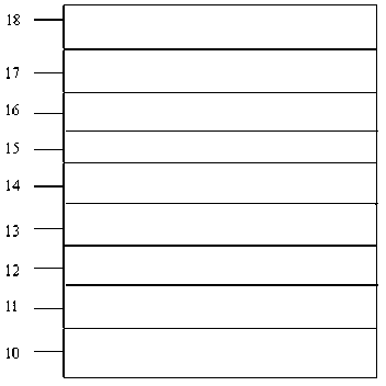
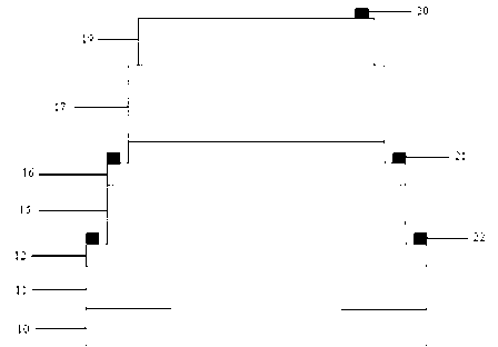
[0056] Specific implementation mode two: In this implementation mode, the Schottky barrier-HEIWIP structure is used as an example for the infrared-ultraviolet dual-color detector (the material structure is as follows: figure 1 and a device structure such as image 3 ), specifically explain the implementation steps of the ultraviolet-infrared dual-color detector. Such as figure 1 Its structure is to sequentially grow a buffer layer 11: ZnO on a sapphire substrate 10 with MOCVD or MBE equipment, with a thickness of 0.02-0.2 μm. The first n-type ohmic contact layer 12: ZnO is grown on the buffer layer 11 with a thickness of 0.5-1 μm and a doping concentration of n ~ scope. On the first n-type ohmic contact layer 12, the first intrinsic layer 13 / heavily doped layer 14 is grown sequentially: i-ZnMgO / n + -ZnO or i-Zn y Mg 1-y O / n + -Znx Mg 1-x O (x>y); the alternately grown first intrinsic layer 13 / heavily doped layer 14 forms a multi-period layer 15, wherein the electron...
specific Embodiment approach 3
[0063] Embodiment 3: The difference between this embodiment and Embodiment 2 is that when the ultraviolet detection adopts the p-i-n structure, then a p-type layer 18 is grown on the second intrinsic layer 17: p-ZnO or p-ZnMgO, empty The hole concentration is to Range, thickness 0.02~0.2 μm, p-i-n—HEIWIP structure such as figure 2 As shown, the device structure is as Figure 4 shown.
PUM
 Abstract
Description
Claims
Application Information


