Ultraviolet and infrared double-color detector and manufacturing method thereof

A two-color detector and infrared technology, applied in semiconductor devices, final product manufacturing, sustainable manufacturing/processing, etc., can solve problems such as inability to detect ultraviolet radiation at the same time

Inactive Publication Date: 2010-10-27
INST OF SEMICONDUCTORS - CHINESE ACAD OF SCI
View PDF2 Cites 18 Cited by
  • Summary
  • Abstract
  • Description
  • Claims
  • Application Information

AI Technical Summary

Problems solved by technology

Limited by the nature of the semiconductor material system itself, these

Method used


Image

  • Ultraviolet and infrared double-color detector and manufacturing method thereof
  • Ultraviolet and infrared double-color detector and manufacturing method thereof
  • Ultraviolet and infrared double-color detector and manufacturing method thereof

Examples


Embodiment

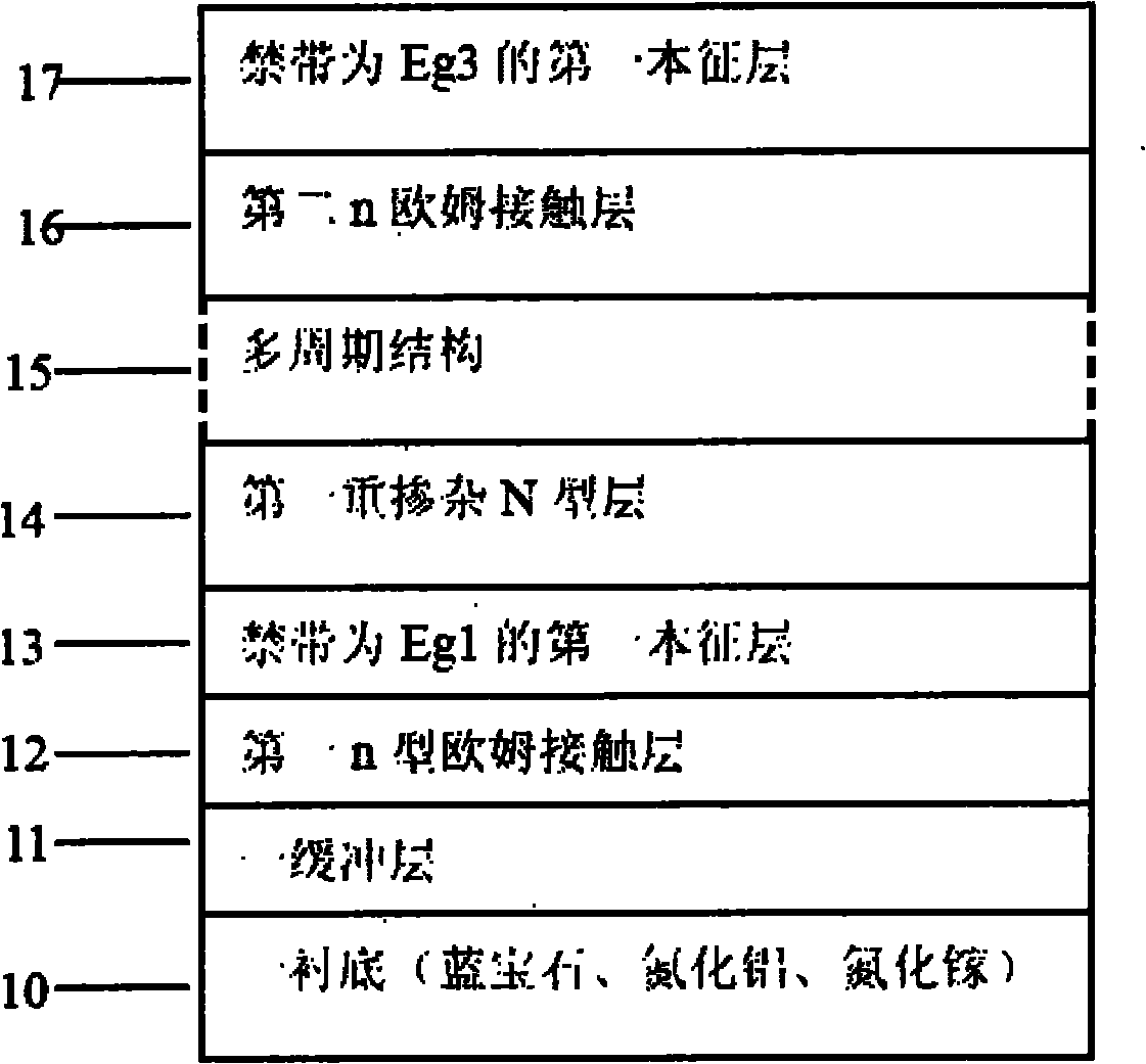
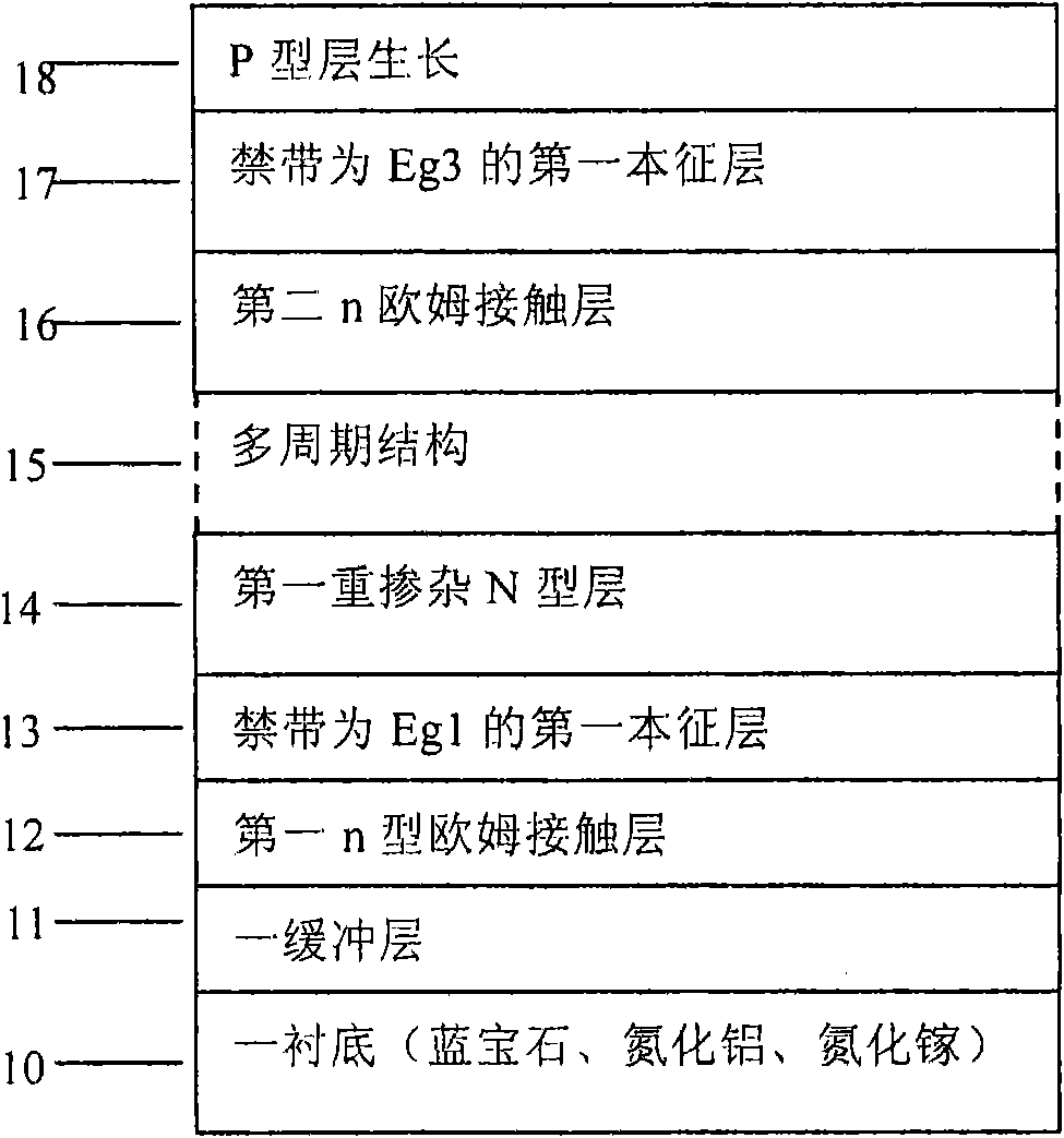
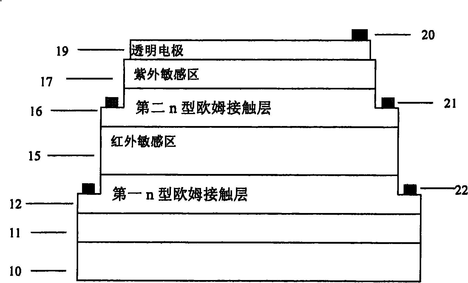
[0089] Taking the Schottky barrier-HEIWIP structure as an example for the infrared-ultraviolet dual-color detector, the structure is to sequentially grow a thin layer of AlN or GaN buffer layer 11 on the sapphire substrate 10 using MOCVD or MBE equipment, with a thickness of 0.02 to 0.1 μm, grow the first n-type ohmic contact layer 12 on the buffer layer 11: n + - AlGaN or GaN, with a thickness of 1.5-5.0 μm and a doping concentration n of 5×10 17 cm -3 ~5×10 19 cm -3 scope. Intrinsic layer 13 / heavily doped layer 14 is sequentially grown on the first n-type ohmic contact layer 12: i-AlGaN / n + -GaN or i-Al x Ga 1-x N / n + -Al y Ga 1-y N(x>y), alternate growth of intrinsic layer l3 / heavily doped layer 14 to form a multi-period structure 15, wherein, i-AlGaN or i-Al x Ga 1-x The electron carrier concentration of N is 5×10 14 ~5×10 17 cm -3 , with a thickness of 0.02-0.4 μm; n + -GaN or n + -Al y Ga 1-y The concentration of N is at 5×10 17 cm -3 ~5×10 19 cm -3...


PUM

PropertyMeasurementUnit
Thicknessaaaaaaaaaa
Thicknessaaaaaaaaaa
Thicknessaaaaaaaaaa

Abstract

The invention discloses an ultraviolet and infrared double-color detector and a manufacturing method thereof. The ultraviolet and infrared double-color detector comprises a substrate, a buffer layer, a first n-type ohmic contact layer, a multicycle layer, a second n-type ohmic contact layer, an intrinsic layer, a transparent electrode, an upper electrode, a middle electrode and a lower electrode, wherein a material structure for the ultraviolet and infrared double-color detector is grown on the substrate; the buffer layer is grown on the substrate; the first n-type ohmic contact layer is grown on the buffer layer for ohmic contact; the multicycle layer is comprised of a first intrinsic layer and a heavily-doped n-type layer, which are grown alternately; the second n-type ohmic contact layer is grown on the multicycle layer and part of the second n-type ohmic contact layer serves as a n-type ohmic contact electrode; the intrinsic layer has a forbidden band width of Eg3 which is less than or equal to Eg2 and is grown on the second n-type ohmic contact layer; the transparent electrode is formed on the intrinsic layer having the forbidden band width of Eg3; the upper electrode is formed in a small area on the transparent electrode; the middle electrode is formed in the electrode window of the second n-type ohmic contact layer; and the lower electrode is formed in the electrode window of the first second n-type ohmic contact layer.

Description

technical field [0001] The invention relates to the technical field of semiconductor photodetectors, in particular to an ultraviolet-infrared dual-color detector and a manufacturing method. Background technique [0002] Most of the response wavelengths of two-color or multi-color semiconductor detectors developed at home and abroad are distributed in the near, middle and far infrared ranges. Limited by the nature of the semiconductor material system itself, these detectors cannot simultaneously detect radiation in the ultraviolet band. [0003] Gallium nitride (GaN) and aluminum nitride (AlN) are direct bandgap semiconductor materials, and the bandgap widths are about 3.4eV and 6.2eV respectively. The forbidden band width of AlGaN alloy material increases with the increase of Al composition, and the corresponding absorption peaks are distributed in the ultraviolet range. use n + -GaN / i-Al(In)GaN or n + -Al y Ga 1-y N / i-Al x Ga 1-x The photoelectron emission effect in...

Claims


Application Information

Patent Timeline
IPC IPC(8): H01L31/101H01L31/0224H01L31/0352H01L31/18
CPCY02P70/50
Inventor 刘宗顺赵德刚朱建军张书明王辉江德生杨辉
Owner INST OF SEMICONDUCTORS - CHINESE ACAD OF SCI
Why Eureka
Try Eureka