
Array substrate and display panel

An array substrate and metal array technology, applied in nonlinear optics, instruments, optics, etc., can solve the problems of large trace impedance and uneven display, and achieve the effect of reducing trace impedance

Pending Publication Date: 2022-07-08
CHUZHOU HKC OPTOELECTRONICS TECH CO LTD +1
View PDF3 Cites 1 Cited by
  • Summary
  • Abstract
  • Description
  • Claims
  • Application Information

AI Technical Summary

Problems solved by technology

[0004] One of the purposes of the embodiments of the present application is to provide an array substrate and a display panel, by arranging multiple dummy lines between multiple metal array lines and multiple fan-out lines to solve the problems in the prior art. The traces close to the edge of the metal array trace and the edge of the fan-out trace are thinner, and the impedance of the trace is relatively large, resulting in the problem of uneven display caused by the difference in impedance

Method used


Image

  • Array substrate and display panel
  • Array substrate and display panel
  • Array substrate and display panel

Examples


Embodiment 1

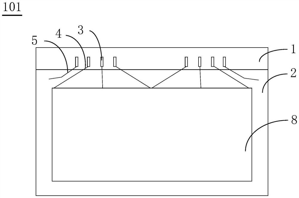
[0038] like figure 1 As shown, the first array substrate 101 provided in the first embodiment of the present application includes a binding area 1 , a non-display area 2 , and a display area 8 .

[0039] The non-display area 2 is located around the display area 8 . The binding pin 3 from the binding area 1 extends to the non-display area 2, respectively, the data signal in the binding pin 3 is connected to the fan-out trace 4, and the GOA signal and the com signal in the binding pin 3 are connected to the WOA Route 5.

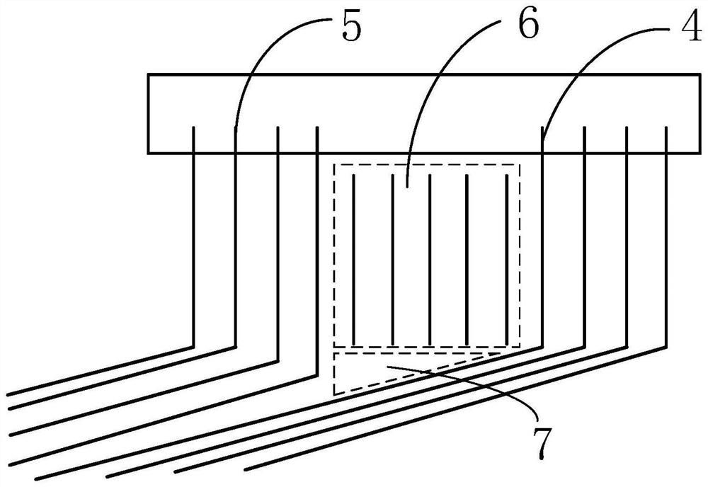
[0040] In the present embodiment, the non-display area 2 is provided with a plurality of WOA lines 5 and a plurality of fan-out lines 4, and the plurality of WOA lines 5 and the plurality of fan-out lines 4 are arranged at intervals from each other. Specifically, the plurality of WOA lines The traces 5 are concentrated in one area, and the multiple fan-out traces 4 are concentrated in another area. There is a large gap between the two areas. The non-display a...

Embodiment 2

[0055] like Figure 4 As shown, the spacing between adjacent virtual traces 6 changes in steps from the side of the plurality of WOA traces 5 to the side of the plurality of fan-out traces 4 .

[0056] In this embodiment, the virtual traces 6 are divided into different gradients, the number of gradients is not limited, the spacing between the virtual traces 6 between different gradients is different, and the spacing between the virtual traces 6 of the same gradient is the same . From one side of the virtual trace 6 to the other side, the length of the spacing changes from large to small, specifically by comparing the spacing between the WOA traces 5 and the fan-out traces 4, when the distance between the WOA traces 5 is greater than the distance between the fan-out traces 4, then the trace spacing of the virtual trace 6 gradient close to the WOA trace 5 side is greater than the trace distance of the virtual trace 6 gradient close to the fan-out trace 4 side, when The distanc...

Embodiment 3

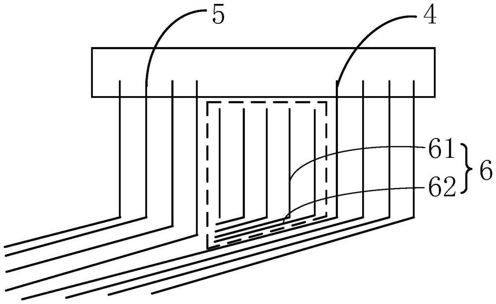
[0060] like Figure 5 As shown, the spacing between the multiple virtual traces 6 changes linearly from one side of the multiple WOA traces 5 to the side of the multiple fan-out traces 4 , that is, the variation of the spacing is extremely small and approximately a continuous change.

[0061] Obtain the spacing between WOA traces 5, and obtain the spacing between fan-out traces 4. The spacing between virtual traces 6 near the metal traces is similar to the spacing between WOA traces 5, and virtual traces 6 are close to the fan-out. The spacing on one side of the line 4 is similar to the distance between the fan-out traces 4 , and the spacing on one side of the virtual trace 6 changes gradually to the spacing between the virtual traces 6 on the other side.

[0062] In other embodiments, while keeping the distance between the dummy traces 6 the same as the distance between the dummy traces 6 in this embodiment, the trace length of the dummy traces 6 may be appropriately extended...


PUM


Abstract

The invention relates to the technical field of display, and provides an array substrate and a display panel, the array substrate is provided with a non-display area, the non-display area is provided with a plurality of metal array wires and a plurality of fan-out wires, the plurality of metal array wires and the plurality of fan-out wires are arranged at intervals, the non-display area is further provided with a plurality of virtual wires, and the plurality of virtual wires are arranged at intervals. The plurality of virtual wires are arranged in an area between the plurality of metal array wires and the plurality of fan-out wires. According to the method, the virtual wires are arranged between the metal array wires and the fan-out wires, so that the wire impedance of the edges of the metal array wires and the fan-out wires is reduced, and the problems that in the prior art, the wires close to the edges of the metal array wires and the fan-out wires are thin, the wire impedance is large, and the wire impedance is large are solved. Therefore, the problem of non-uniform display caused by impedance difference is solved.

Description

technical field [0001] The present application belongs to the field of display technology, and relates to an array substrate and a display panel. Background technique [0002] In the liquid crystal display panel, there are an array substrate and a color filter substrate. The formation of each layer pattern on the array substrate and the fabrication process of each layer of the array pattern require film deposition, cleaning, photoresist coating, exposure, and development. , etching, photoresist stripping and inspection of these 8 process steps. [0003] In the prior art, the bonding area of ​​the panel is connected with fan-out wiring and WOA wiring, the fan-out wiring is connected with the data signal line in the bonding area, and the WOA wiring is connected with the driving signal line and the common wiring in the bonding area. Because of the difference in the number of connected pins on the binding area, when the fan-out trace and the WOA trace introduce valid signals on...

Claims


Application Information

Patent Timeline
Patent Type & Authority Applications(China)
IPC IPC(8): G02F1/1362
CPCG02F1/136286
Inventor 常红燕袁海江
Owner CHUZHOU HKC OPTOELECTRONICS TECH CO LTD
Learn More