Power semiconductor device

A semiconductor and power technology, applied in the field of power semiconductor devices, can solve problems such as reduced insulation and achieve the effect of miniaturization

Pending Publication Date: 2022-07-08
MITSUBISHI ELECTRIC CORP
View PDF2 Cites 0 Cited by
  • Summary
  • Abstract
  • Description
  • Claims
  • Application Information

AI Technical Summary

Problems solved by technology

However, since this structure arranges the main electrode emitter sensing terminal outside the module, there is a concern that the insulation will be reduced.
In addition, from the viewpoint of workability, there is also a problem that the main electrode emitter sense terminal needs to be externally connected to the module.

Method used


Image

  • Power semiconductor device
  • Power semiconductor device
  • Power semiconductor device

Examples


Embodiment Construction

[0022] Hereinafter, embodiments of the present invention will be described based on the drawings.

[0023]

[0024] The technology related to the embodiment of the present invention will be described.

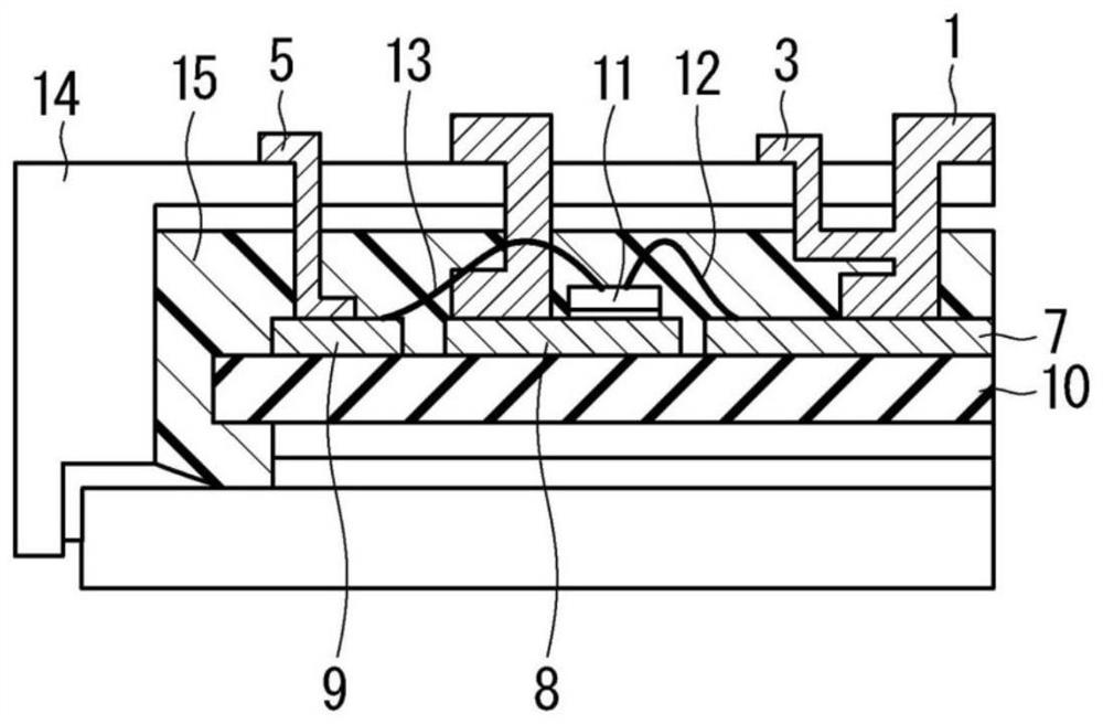
[0025] Figure 7 It is a cross-sectional view showing an example of the structure of a power semiconductor device according to the related art.

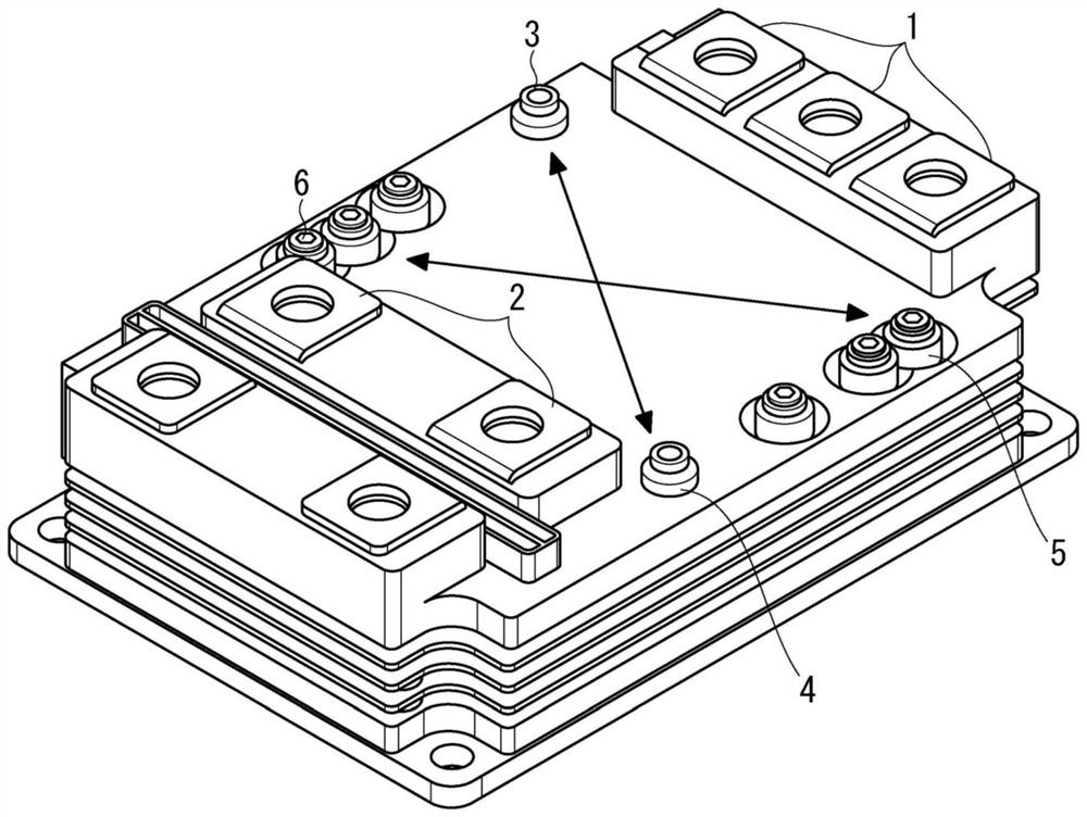
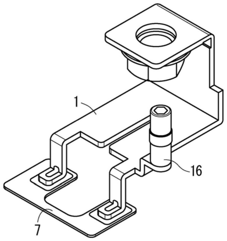
[0026] like Figure 7 As shown, metal patterns 7 , 8 , 9 are provided on top of insulating material 10 . In addition, the metal patterns 7, 8, 9 correspond to the circuit pattern demonstrated above. The emitter main electrode 1 and the main electrode emitter sensing terminal 22 are disposed on the metal pattern 7 . A semiconductor chip 11 is provided over the metal pattern 8 . An auxiliary emitter sensing terminal 5 is provided on the metal pattern 9 .

[0027] The metal pattern 7 is connected to the main electrode of the semiconductor chip 11 , that is, the emitter electrode via the bonding wire 12 . The metal pattern 9 is c...


PUM


Abstract

The purpose of the present invention is to provide a power semiconductor device capable of reducing the size of a module. This power semiconductor device is provided with: emitter main electrodes (1, 2) provided on each of a plurality of semiconductor chips (11); and main electrode emitter sensing terminals (3, 4) which are directly connected to the emitter main electrodes (1, 2), are partially exposed to the outside of the module, and are positioned diagonally in plan view of the outside of the module. The distance between the main electrode emitter sensing terminals (3, 4) and the emitter main electrodes (1, 2) to which the main electrode emitter sensing terminals (3, 4) are connected is closer than the distance between the main electrode emitter sensing terminals (3, 4).

Description

technical field [0001] The present invention relates to a power semiconductor device used for electric motor control of equipment for electrified railways or equipment for automobiles, for example. Background technique [0002] In a power semiconductor device, there is a method of performing control such as short-circuit protection based on the difference between the inductances of the main electrode emitter electrode and the auxiliary emitter electrode. A conventional power semiconductor device has a structure in which a main electrode emitter sensing terminal is connected to a circuit pattern on an insulating substrate provided inside the module, and a part of the main electrode emitter sensing terminal is drawn out to the circuit pattern. outside of the module. However, this structure has problems such as complicated wiring and limited space above the insulating substrate. [0003] In addition, along with the miniaturization of the module, a structure in which the main ...

Claims


Application Information

Patent Timeline
Patent Type & Authority Applications(China)
IPC IPC(8): H01L25/07
CPCH01L2224/48227H01L2224/32225H01L2224/73265H01L2924/181H01L25/072H01L2924/00012H01L2924/00
Inventor 大宅大介林田幸昌本宫哲男
Owner MITSUBISHI ELECTRIC CORP
Why Eureka
Try Eureka