LED packaging structure and preparation method of LED packaging structure

A technology of LED packaging and LED chips, applied in semiconductor devices, electrical components, circuits, etc., can solve problems such as the inability to achieve a 180° light-emitting angle and a small light-emitting angle

Pending Publication Date: 2022-07-15
SHENZHEN JUFEI OPTOELECTRONICS CO LTD
View PDF0 Cites 1 Cited by
  • Summary
  • Abstract
  • Description
  • Claims
  • Application Information

AI Technical Summary

Problems solved by technology

[0003] The technical problem to be solved by the present invention is that the light-emitting angle of the current LED devices is small, generally only about 120°, and cannot reach the light-emitting angle of 180°

Method used


Image

  • LED packaging structure and preparation method of LED packaging structure
  • LED packaging structure and preparation method of LED packaging structure
  • LED packaging structure and preparation method of LED packaging structure

Examples


Embodiment 1

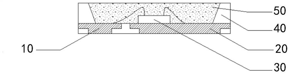
[0041] For LED devices, the light-emitting angle is a very important parameter. The larger the light-emitting angle, the wider the illumination area of ​​an LED device and the more areas that can be illuminated. The current LED device has a light-emitting angle of an LED lamp. The maximum can only reach about 120°, and it is almost impossible to reach 180°. Therefore, in view of the above problems, the application provides an LED package structure, so that the light-emitting angle of an LED lamp can reach 180°, and it can also ensure that each The brightness of the angle is close.

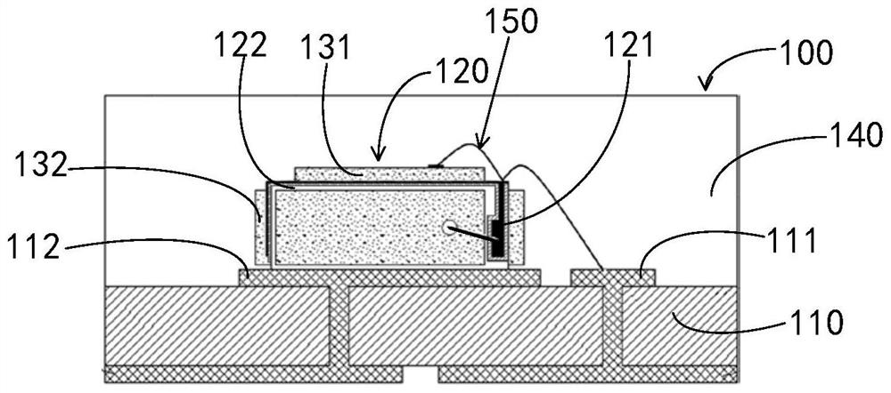
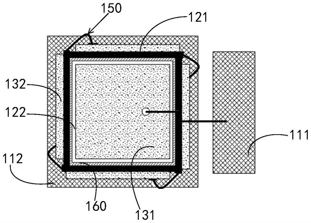
[0042] This embodiment provides an LED package structure, including: a substrate, on which a first pad and a second pad are arranged; a carrier, where the bottom surface of the carrier is fixed on the substrate, and the carrier is There are third pads and fourth pads, the third pads configured to partially cover the top surface of the carrier and extending to each side, the fourth pads configured t...

Embodiment 2

[0064] This embodiment also provides a preparation method of the LED packaging structure, and the preparation method of the LED packaging structure includes:

[0065] S01: A substrate and a carrier are provided, a first pad and a second pad are arranged on the substrate, a third pad and a fourth pad are arranged on the carrier, and the third pad is configured to partially cover the top surface of the carrier and extending to each side, the fourth pad being configured to partially or fully cover the top surface of the carrier and extending to each side and bottom;

[0066] S02: the carrier is fixed on the substrate, and the fourth pad on the bottom surface of the carrier is welded to the second pad of the substrate;

[0067] S03: Weld and fix the LED chip on each surface of the carrier except the bottom surface, the LED chip is a vertical structure chip, and the bottom electrode of the LED chip is bonded and welded on the fourth pad on the surface where it is located;

[0068]...


PUM

PropertyMeasurementUnit
beam angleaaaaaaaaaa

Abstract

The embodiment of the invention provides an LED packaging structure and a preparation method of the LED packaging structure, and the LED packaging structure comprises a substrate which is provided with a first bonding pad and a second bonding pad; the bottom surface of the carrier is fixed on the substrate, the carrier is provided with a third bonding pad and a fourth bonding pad, the third bonding pad is configured to partially cover the top surface of the carrier and extend to each side surface, the fourth bonding pad is configured to partially or completely cover the top surface of the carrier and extend to each side surface, the third bonding pad is electrically connected with the first bonding pad, and the fourth bonding pad is electrically connected with the second bonding pad. The fourth bonding pad is electrically connected with the second bonding pad; the plurality of LED chips are respectively fixed on each surface, except the bottom surface, of the carrier; and the protective colloid covers the substrate, the carrier and the plurality of LED chips. According to the LED device, the carrier is arranged, and the LED chips are respectively welded on each surface of the carrier, so that the light-emitting angle of one LED device reaches 180 degrees, and the light-emitting angle of the LED device and the light-emitting brightness of each angle are obviously improved.

Description

technical field [0001] The invention relates to the technical field of LEDs, and more particularly, to an LED packaging structure and a preparation method of the LED packaging structure. Background technique [0002] Commonly used LED chips, generally 90% of the light is emitted from the front, and only about 10% of the light is emitted from the side, so the light-emitting angle of the LED chip is generally 120°. The common structure is to fix the LED chip in a bracket with a cup, and perform processes such as wire bonding and dispensing, so that the LED device is finally formed. figure 1 It is a common LED packaging structure, and the LED packaging structure includes: LED positive electrode 10 , LED negative electrode 20 , LED chip 30 , LED bracket 40 and protective glue 50 . Since the angle of the chip is only about 120°, the light-emitting angle of the LED device is generally 120° to 130° due to the barrier of the bracket bowl and the refraction of the packaging glue aft...

Claims


Application Information

Patent Timeline
Patent Type & Authority Applications(China)
IPC IPC(8): H01L25/075H01L33/62H01L33/54
CPCH01L25/0753H01L33/62H01L33/54H01L2933/0033H01L2933/005
Inventor 邢美正魏冬寒
Owner SHENZHEN JUFEI OPTOELECTRONICS CO LTD
Why Eureka
Try Eureka