Hybrid stacked filter chip and manufacturing process thereof

A manufacturing process and filter technology, applied in the field of hybrid stacked filter chips and their manufacturing processes, can solve the problem that filter chips cannot handle sound waves in different frequency bands, and achieve the effect of small size design and high Q value design

Pending Publication Date: 2022-08-05
XWAVE TECH (SHANGHAI) CO LTD
View PDF0 Cites 0 Cited by
  • Summary
  • Abstract
  • Description
  • Claims
  • Application Information

AI Technical Summary

Problems solved by technology

[0005] The purpose of the embodiments of the present invention is to provide a hybrid stacked filter chip and its manufacturing process, aiming to solve the problem that the existing filter chips cannot handle sound waves of different frequency bands

Method used


Image

  • Hybrid stacked filter chip and manufacturing process thereof
  • Hybrid stacked filter chip and manufacturing process thereof
  • Hybrid stacked filter chip and manufacturing process thereof

Examples


Embodiment Construction

[0027] In order to make the objectives, technical solutions and advantages of the present invention clearer, the present invention will be further described in detail below with reference to the accompanying drawings and embodiments. It should be understood that the specific embodiments described herein are only used to explain the present invention, but not to limit the present invention.

[0028] It will be understood that the terms "first", "second" and the like used in this application may be used herein to describe various elements, but these elements are not limited by these terms unless otherwise specified. These terms are only used to distinguish a first element from another element. For example, a first xx script could be referred to as a second xx script, and similarly, a second xx script could be referred to as a first xx script, without departing from the scope of this application.

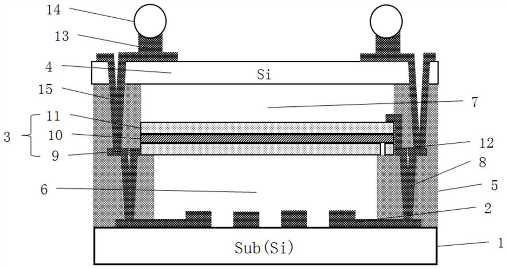
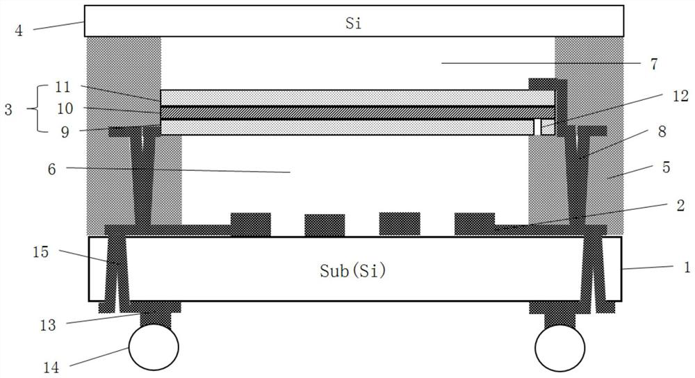
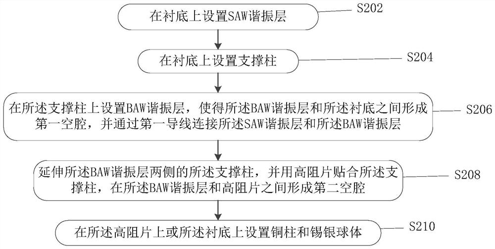
[0029] like figure 1 and 2 As shown, in one embodiment, a hybrid stacked filter...


PUM


Abstract

The invention is suitable for the technical field of MEMS chip manufacturing, and provides a hybrid stacked filter chip. The hybrid stacked filter chip comprises a substrate, an SAW resonance layer, a BAW resonance layer and a high-resistance sheet which are arranged in sequence. The BAW resonance layer is arranged between the substrate and the high-resistance sheet through supporting columns, a first cavity is formed between the BAW resonance layer and the substrate, and a second cavity is formed between the BAW resonance layer and the high-resistance sheet; the SAW resonance layer is arranged in the first cavity and is connected with the BAW resonance layer through a first wire. The substrate, the SAW resonance layer, the BAW resonance layer and the high-resistance sheet are longitudinally stacked to form a laminated module structure, so that requirements of different filtering frequency bands are met, and relatively high Q value design and smaller size design are achieved.

Description

technical field [0001] The invention belongs to the technical field of MEMS chip manufacturing, and in particular relates to a hybrid stacked filter chip and a manufacturing process thereof. Background technique [0002] With the rapid development of today's integrated circuits, large-scale integrated circuits have gradually appeared in people's field of vision. At the same time, with the advancement of the technological era, electronic technology equipment such as mobile phones and automatic vehicles have also appeared one by one, and 5G signals have also been designed accordingly. come out. The advantage of its 5G signal over the original 4G signal is that its frequency band will be larger and wider, the signal transmission will run faster, and the out-of-band frequency band will have a stronger suppression capability. [0003] At present, the classification of filter chips can be divided into SAW type and BAW type. SAW, that is, surface acoustic resonator (Surface Acous...

Claims


Application Information

Patent Timeline
Patent Type & Authority Applications(China)
IPC IPC(8): H03H9/64H03H3/08B81C1/00B81B7/02B81B7/00
CPCH03H9/64H03H3/08B81B7/02B81B7/007B81B7/0045B81C1/00301B81C2203/01
Inventor 胡孝伟代文亮张竞颢崔云辉黄志远
Owner XWAVE TECH (SHANGHAI) CO LTD
Why Eureka
Try Eureka