Auxiliary designing method of contact hole photoetching
An auxiliary design and hole technology, which is applied in the auxiliary design field of contact hole lithography, can solve the problem of shallow focus depth, and achieve the effect of increasing the focal length depth and correcting the optical proximity effect.
- Summary
- Abstract
- Description
- Claims
- Application Information
AI Technical Summary
Problems solved by technology
Method used
Image

Examples
Embodiment 1
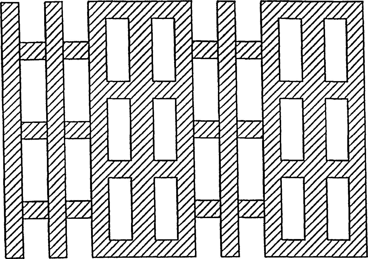
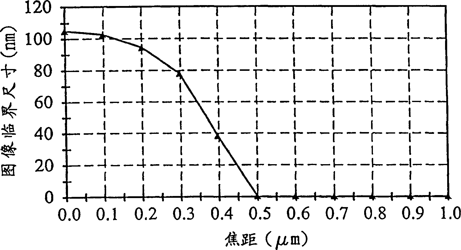
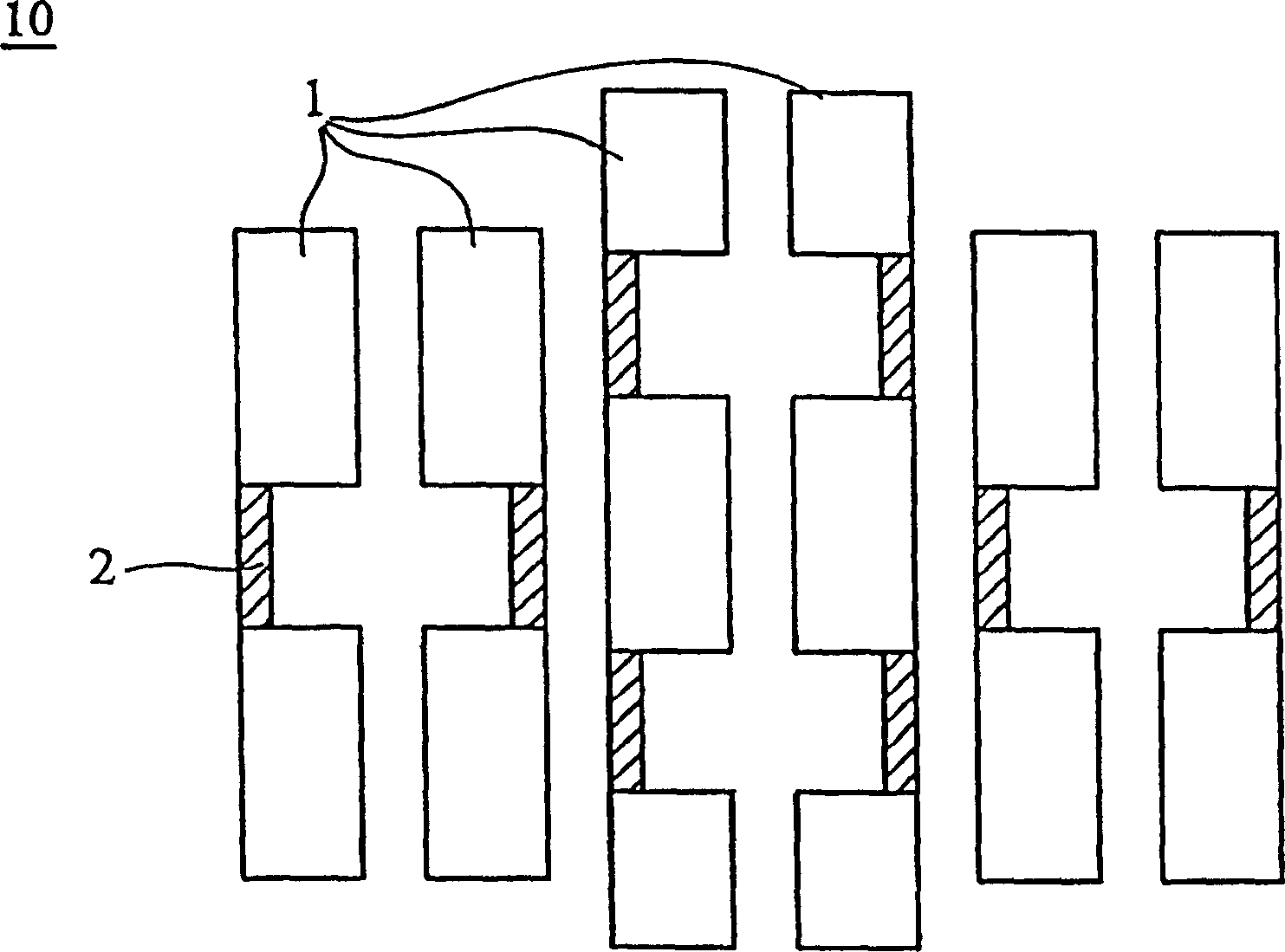
[0032] Figure 2B to Figure 2D These are the size and focal length diagrams of contact holes of different chain types after exposure through the 2 / 3 ring filter of the off-axis illumination system. Figure 2B There are multiple hole patterns on the photomask, and the multiple hole patterns are connected by a line pattern with a line width of 200 nm. Figure 2C There are multiple hole patterns on the photomask, and the multiple hole patterns are connected by a line pattern with a line width of 240 nm. Figure 2D There are multiple hole patterns on the photomask, and the multiple hole patterns are connected by a line pattern with a line width of 280 nm.
[0033] refer to Figure 2B to Figure 2D , as the line width of the linear pattern connecting multiple contact holes in series increases, the focal depth of the contact holes formed by the exposure machine also increases. In the first embodiment, because the line width of the line pattern connecting the plurality of contact h...
Embodiment 2
[0035] Figure 2E to Figure 2G are the focal distance diagrams showing the size and focal length of contact holes of different chain types after exposure through the on-axis fan-shaped filter of the off-axis illumination system. Figure 2E There are multiple hole patterns on the photomask, and the multiple hole patterns are connected by a line pattern with a line width of 200 nm. Figure 2F There are multiple hole patterns on the photomask, and the multiple hole patterns are connected by a line pattern with a line width of 240 nm. Figure 2G There are multiple hole patterns on the photomask, and the multiple hole patterns are connected by a line pattern with a line width of 280 nm.
[0036] refer to Figure 2E to Figure 2G , as the line width of the linear pattern connecting multiple contact holes in series increases, the focal depth of the contact holes formed by the exposure machine also increases. In the second embodiment, because the line width of the line pattern conne...
PUM
 Abstract
Description
Claims
Application Information
 - R&D Engineer
- R&D Manager
- IP Professional
- Industry Leading Data Capabilities
- Powerful AI technology
- Patent DNA Extraction
Browse by: Latest US Patents, China's latest patents, Technical Efficacy Thesaurus, Application Domain, Technology Topic.
© 2024 PatSnap. All rights reserved.Legal|Privacy policy|Modern Slavery Act Transparency Statement|Sitemap