Image display device

A technology for image display devices and bus electrodes, which is applied in the direction of image/graphic display tubes, electrode devices and related components, screen tubes, etc., and can solve problems such as increased step difference, increased film resistance value, and disconnection

Inactive Publication Date: 2007-02-21
HITACHI LTD
View PDF4 Cites 0 Cited by
  • Summary
  • Abstract
  • Description
  • Claims
  • Application Information

AI Technical Summary

Problems solved by technology

For this problem, the existing structure has the problem of insufficient oxidation resistance of the thin upper bus electrode lower layer 16
For example, W is a material that is relatively easily oxidized. When the film thickness is as thin as about 10 nm, it is almost completely oxidized by heating at 400°C or higher, and the sheet resistance value increases rapidly, making it difficult to obtain electrical contact with the upper electrode 13.
If the film thickness is more than 20nm, the surface oxide film inhibits the diffusion of oxidized species, prevents the overall oxidation and maintains low resistance, but the step difference becomes larger, which reduces the reliability of electrode connection
[0008] Another problem is the disconnection of the thin upper bus electrode lower layer 16 due to the thermal stress caused by the high temperature heat treatment of the frit glass seal

Method used


Image

  • Image display device
  • Image display device
  • Image display device

Examples


no. 1 Embodiment

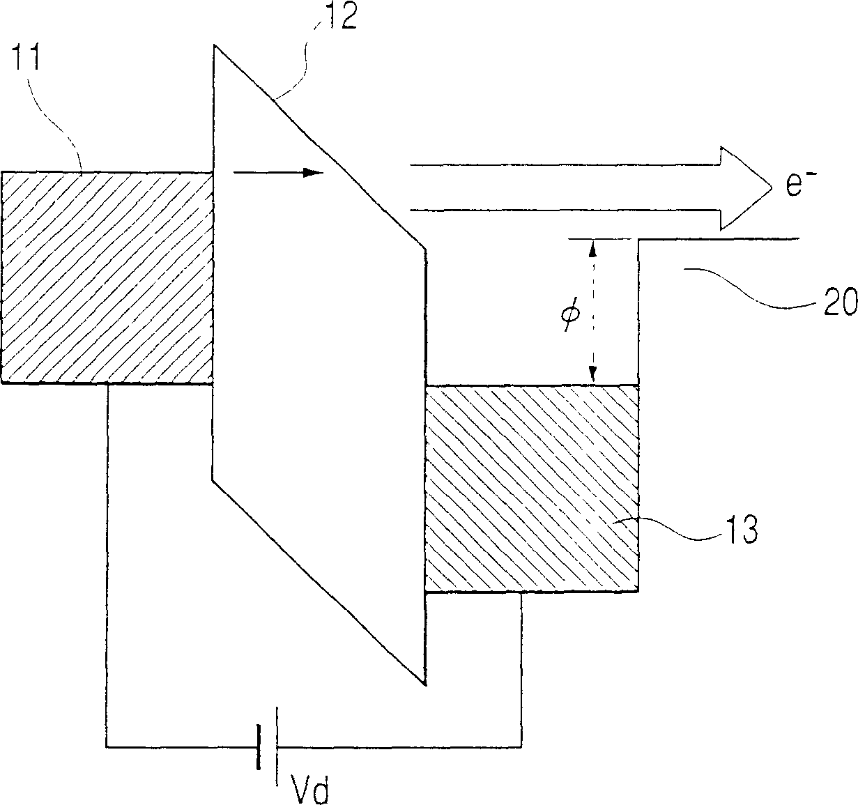
[0043] As the first embodiment of the present invention to achieve the above object, taking the MIM type as an example, it is described that the upper part is formed by stacking the first metal layer (upper bus electrode), the second metal layer, and the insulating layer in this order from the upper bus electrode. Thin-film electron source (cathode) in case of laminated film of bus electrode and overhang structure.

[0044] First, use Figure 4-15 A method of forming a thin-film electron source will be described.

[0045] First, a metal film for the lower electrode is formed on an insulating substrate 10 such as glass. As the lower electrode material, Al and Al alloys are used. The reason why Al and Al alloys are used is that a high-quality insulating film can be formed by anodic oxidation. Here, an Al—Nd alloy doped with 2 atomic weight % of Nd was used. For film formation, for example, a sputtering method is used. The film thickness was 300 nm. After film formation, th...

no. 2 Embodiment

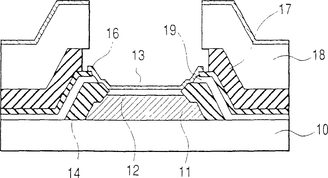
[0058] As a second embodiment of the present invention that achieves the above object, the MIM type is used as an example to explain that the laminated film constituting the upper bus electrode and the overhang structure is that the first metal layer (upper bus electrode) is sequentially laminated from the upper bus electrode side. ), an insulating layer, and a thin-film electron source in the case of a second metal layer (surface electrode).

[0059] First, the electron acceleration layer 12 was formed according to the same procedure as in Example 1. Next, the second protective insulating layer 19 and the first metal layer 26 are formed into films. As the second protective insulating layer 19 , for example, Si oxide is used, and the film thickness is 40 nm. On the other hand, as the material of the first metal layer 26, an Al—Nd alloy is used. In addition, as the first metal layer 26, Cr or a Cr alloy or the like may be used. The film thickness is 300nm ( Figure 16 ).

...

no. 3 Embodiment

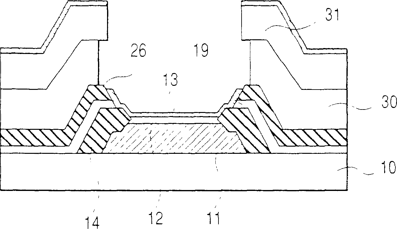
[0067] As a third embodiment of the present invention that achieves the above object, the MIM type is used as an example to explain that the laminated film constituting the upper bus electrode and the overhang structure is that the first metal layer (upper bus electrode) is sequentially laminated from the upper bus electrode side. ), a thin-film electron source in the case of the first insulating layer and the second insulating layer.

[0068] First, the first metal layer (upper bus electrode) 26 is processed and formed so as to be perpendicular to the lower electrode 11 by the same procedure as in the second embodiment. Here, an Al—Nd alloy is used as the material of the first metal layer 26 . In addition, Cr or a Cr alloy or the like may be used as the first metal layer. The film thickness is 300nm ( Figure 17 ).

[0069] Next, the first insulating layer 30 and the second insulating layer 31 which are laminated films of the overhang structure are formed ( Figure 23 ). ...


PUM


Abstract

The invention provides an image display device capable of realizing a high reliabiliby of wiring connection of a top electrode. The image display device comprises a substrate having a base electrode, a top electrode, and an electron acceleration layer disposed between the base electrode and the top electrode, which substrate is formed of arrayed thin film cathodes that emit electrons from the top electrode side by applying a voltage between the base electrode and the top electrode; and a phosphor screen, wherein the arrayed thin film cathodes have a top bus electrode served as a current feed line to the top electrode, which top bus electrode is tapered so that the film thickness decreases toward an electron emission portion side, and have an overhang structure that separates the top electrode into individual cathodes.

Description

technical field [0001] The present invention relates to an image display device including: a lower electrode and an upper electrode; An electron accelerating layer is formed, and electrons are emitted from the upper electrode after a voltage is applied between the lower electrode and the upper electrode; and a fluorescent surface. Background technique [0002] The thin-film electron source is based on a laminated structure of three thin films: an upper electrode, an electron acceleration layer, and a lower electrode. A voltage is applied between the upper electrode and the lower electrode, and electrons are emitted from the surface of the upper electrode into vacuum. For example, there are MIM (Metal-Insulator-Metal) type in which metal-insulator-metal is laminated, metal-insulator-semiconductor type, and the like. Regarding the MIM type, for example, it is disclosed in (Japanese) Unexamined Patent Application No. 7-65710, and regarding the metal-insulator-semiconductor typ...

Claims


Application Information

Patent Timeline
Patent Type & Authority Patents(China)
IPC IPC(8): H01J31/12H01J29/02H01J29/46H01J9/02H01J1/312H01J29/04
CPCH01J31/127B82Y10/00H01J1/312H01J9/02
Inventor 楠敏明佐川雅一铃木睦三
Owner HITACHI LTD
Why Eureka
Try Eureka