Ic card and manufacturing method thereof

一种集成电路卡、图形的技术,应用在印刷电路制造、印刷、仪器等方向,能够解决难制造超耐用性触点焊盘和芯片模块等问题

Inactive Publication Date: 2007-03-14
SAMSUNG TECHWIN CO LTD
View PDF5 Cites 2 Cited by
  • Summary
  • Abstract
  • Description
  • Claims
  • Application Information

AI Technical Summary

Problems solved by technology

Also, due to the arrangement of chips or chip modules and external contact pads in a card of limited thickness, it is difficult to manufacture ultra-durable contact pads and chip modules

Method used


Image

  • Ic card and manufacturing method thereof
  • Ic card and manufacturing method thereof
  • Ic card and manufacturing method thereof

Examples


Embodiment Construction

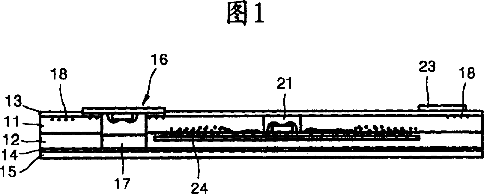
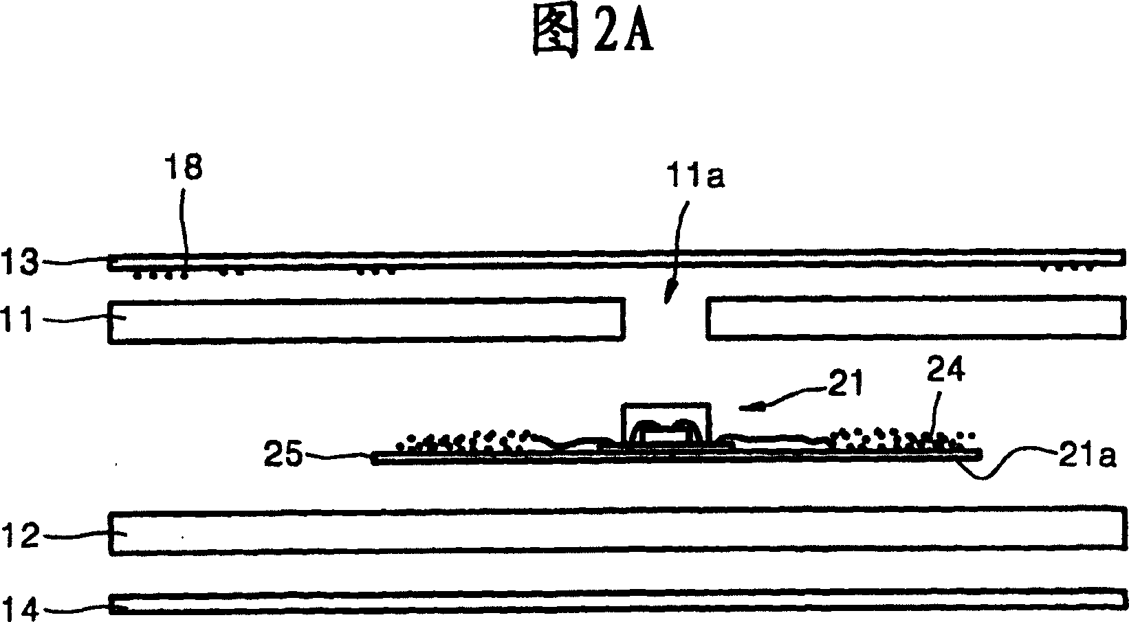
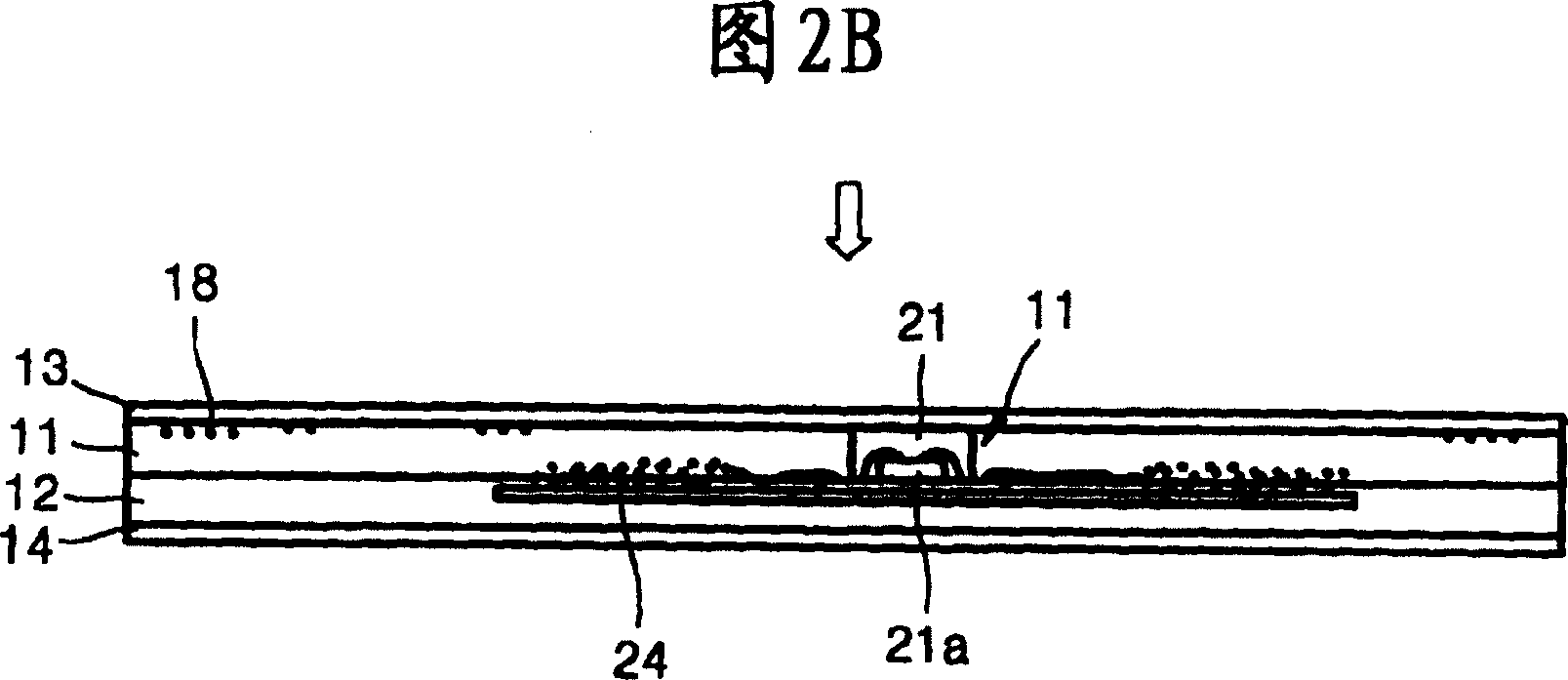
[0033] Referring to FIG. 3A, a clad layer 31 made of copper is formed on the film 32. Referring to FIG. The cover layer 31 is provided as a conductive layer to form a high-frequency antenna pattern and a pattern for connecting contact terminals (not shown).

[0034] Referring to FIG. 3B, a coating 31 to be formed into a predetermined antenna circuit pattern 31' is formed on the film 32. Referring to FIG. The antenna circuit pattern 31' can be formed by a typical method. For example, a photoresist is coated on the cladding layer 31, and then covered with a photomask. The photoresist is exposed and developed in this state, and then the cladding layer 31 is etched. An antenna pattern is then formed by removing the photoresist. The antenna circuit pattern includes a linear antenna portion 31a formed in a ring shape, a portion 31b corresponding to a chip bump (not shown) of the composite chip, and an attachment portion 31c to which the external contact pad 45 shown in FIG. 3K is...


PUM


Abstract

An IC card includes an antenna circuit pattern formed on an insulation film and having a wire-shaped antenna portion, a portion corresponding to a chip bump of a combi-chip, and an attachment portion to which an external contact pad is attached. The combi-chip is attached to a portion corresponding to the chip bump of the combi-chip module on the antenna circuit pattern. At least one dielectric layer is attached to the antenna circuit pattern. An external contact pad is inserted in a hole formed in part of the dielectric layer and attached to the hole and has terminals formed in an outer surface and an inner surface of a substrate and connected to one another. The terminals on the inner surface contact the attachment portion is provided on the antenna circuit pattern.

Description

[0001] This application claims priority from Korean Patent Application 2002-32517 filed with the Korean Intellectual Property Office on June 11, 2002, the disclosure of which is incorporated herein by reference in its entirety. technical field [0002] The present invention relates to an IC card and its manufacturing method, and more particularly, to an IC card and its manufacturing method in which an antenna circuit board and a contact circuit board of a composite chip provided in the IC card are directly connected so as to reduce resistance. Background technique [0003] An IC card refers to a card on which an IC chip is mounted, and can be used as an electronic ID card, a license card, electronic money, and a credit card by inputting various information into the IC chip. For example, an IC card can be used as an electronic ID card by inputting personal information such as address, name, civil registration number (or ID number) information, driver's license number, medical ...

Claims


Application Information

Patent Timeline
Patent Type & Authority Patents(China)
IPC IPC(8): G06K19/07B42D15/10G06K19/077H01L25/00H05K1/11H05K1/14H05K3/28
CPCG06K19/07749H01L2224/16227H01L2224/83192H05K3/284H01L2224/73204G06K19/0775H05K1/141H01L2224/32225H01L2224/45139H01L2924/01087G06K19/07769H01L2224/48091H05K1/11H01L2224/16225G06K19/07745H01L2924/3025H01L2924/01078H01L2224/48227H01L2924/01068H01L2924/01079H01L2924/00011H01L2924/00014H01L2924/00H01L2924/01049H01L2224/45015H01L2924/207G06K17/00
Inventor 金德兴金昌圭李升燮
Owner SAMSUNG TECHWIN CO LTD
Why Eureka
Try Eureka