
Fuse circuit used for semiconductor integrated circuit

An integrated circuit and semiconductor technology, applied in the direction of semiconductor devices, circuits, semiconductor/solid-state device components, etc., can solve the problems of fuse cutting technology difficulties, lower product qualification rate, increase semiconductor storage devices, etc., to reduce programming defects , The effect of reducing the defect generation rate

Inactive Publication Date: 2002-05-15
SAMSUNG ELECTRONICS CO LTD
View PDF1 Cites 13 Cited by
  • Summary
  • Abstract
  • Description
  • Claims
  • Application Information

AI Technical Summary

Problems solved by technology

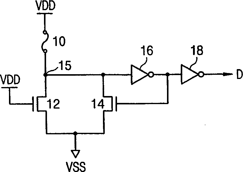
As the density of semiconductor memory devices increases and the layout size of circuit elements containing fuses decreases proportionally, the cutting technology of fuses becomes more and more difficult
Incorrect (or failed) cutting of the fuse leads to invalid programming in the fuse circuit, resulting in a reduction in product yield

Method used


Image

  • Fuse circuit used for semiconductor integrated circuit
  • Fuse circuit used for semiconductor integrated circuit
  • Fuse circuit used for semiconductor integrated circuit

Examples


Embodiment Construction

[0023] It should be understood that the following description of the preferred embodiments is for illustration only and not in a limiting sense. In the following detailed description, certain details are set forth in order to provide a thorough understanding of the present invention. However, it will be apparent to one skilled in the art that the present invention may be practiced without these specific details.

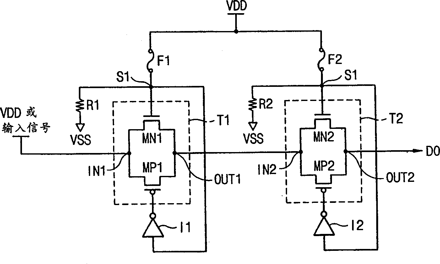
[0024] figure 2 is a circuit diagram of a fuse circuit according to an embodiment of the present invention.

[0025] refer to figure 2 , The fuse circuit is composed of fuses F1 and F2, transmission gating circuits T1 and T2, inverters I1 and I2, and resistors R1 and R2. Fuses F1 and F2 are made of polysilicon, or other laser cuttable metal materials such as titanium (Ti) or titanium nitride (TiN). Each fuse F1 and F2 is connected between a power supply voltage VDD and detection nodes S1 and S2. The transmission gate circuit T1 is connected to the fuse F1, and...


PUM


Abstract

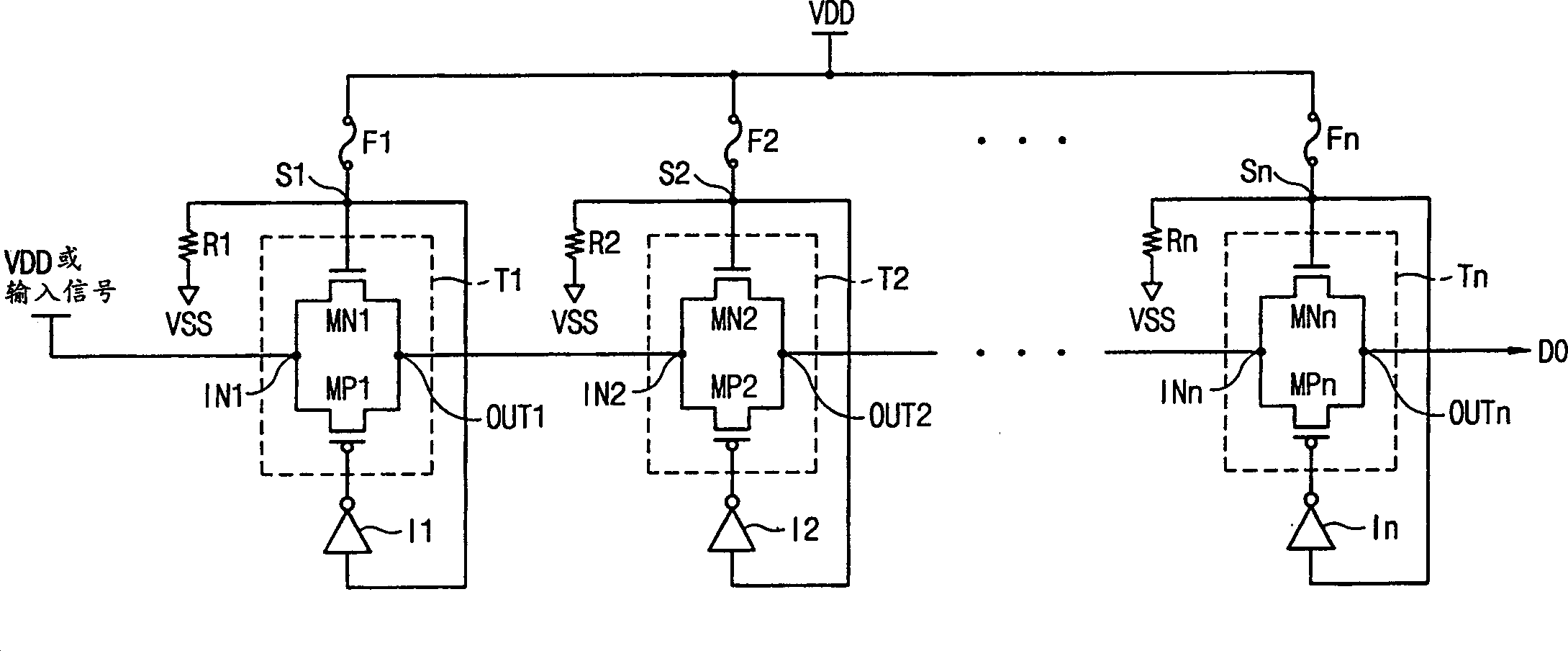
In a fuse circuit including programmable fuses in a semiconductor integrated circuit, the fuses store specific information related to the semiconductor integrated circuit, such as redundancy information, wafer lot number, die lot number, and die position on the wafer, etc. While a conventional semiconductor integrated circuit utilizes a single fuse for storing one bit of specific information, the fuse circuit in the present invention utilizes a plurality of fuses for storing identical bit information. Consequently, in the case where a fuse has not been cut out correctly, the fuse circuit of the present invention can reduce programming defects, whereby defect generation rates are remarkably decreased.

Description

[0001] This application is based on the priority of Korean Patent Application No. 2000-61257 filed on October 18, 2000, the contents of which are incorporated herein by reference in their entirety. technical field [0002] The present invention relates generally to semiconductor integrated circuit devices, and more particularly to a fuse circuit for use in semiconductor integrated circuits. Background technique [0003] While the storage capacity of integrated circuit memory continues to increase by increasing the level of integration, the defects of corresponding memory cells (cells) increase, which is due to the increase in the complexity of the manufacturing process, resulting in a decrease in product yield. In general, it is difficult to make a memory device free of defective cells. Therefore, various efforts are being made to improve the yield of highly integrated memory devices. [0004] It is best to improve the manu...

Claims


Application Information

Patent Timeline
Patent Type & Authority Applications(China)
IPC IPC(8): G11C29/00G11C17/16
CPCG11C17/16G11C29/00
Inventor 郑苍焕金殷汉
Owner SAMSUNG ELECTRONICS CO LTD
Learn More