
Fuse circuit for semiconductor integrated circuit

Inactive Publication Date: 2005-01-04
SAMSUNG ELECTRONICS CO LTD
View PDF7 Cites 11 Cited by
  • Summary
  • Abstract
  • Description
  • Claims
  • Application Information

AI Technical Summary

Benefits of technology

It is therefore an object of the present invention to provide a fuse circuit embedded in semiconductor integrated circuits capable of reducing programming defects, even in the case where a fuse has not been cut out correctly.
According to the fuse circuit of the invention, the fuse circuit is able to reduce programming defects, even in cases where the fuses have not been cut out correctly. Thereby, defect generation rates are remarkably decreased.

Problems solved by technology

As the storage capacity of integrated circuit memories continues to increase through higher integration, associated memory cell defects rise accordingly, due to increased complexity in manufacturing processes, leading to degradation of production yield.
In general, it is difficult to render a memory device having no defective cells.
As semiconductor memory device density is increased to scale down topological size of circuit elements including the fuses, the cut out technique for the fuses becomes more and more of a challenge.
An incorrect (or failed) cut out of the fuses results in an invalid programming in the fuse circuit, causing degradation of the production yield.

Method used


Image

  • Fuse circuit for semiconductor integrated circuit
  • Fuse circuit for semiconductor integrated circuit
  • Fuse circuit for semiconductor integrated circuit

Examples


Embodiment Construction

It should be understood that the following description of preferred embodiments is merely illustrative and that it should not be taken in a limiting sense. In the following detailed description, several specific details are set forth in order to provide a thorough understanding of the present invention. It will be apparent, however, to one skilled in the art, that the present invention may be practiced without these specific details.

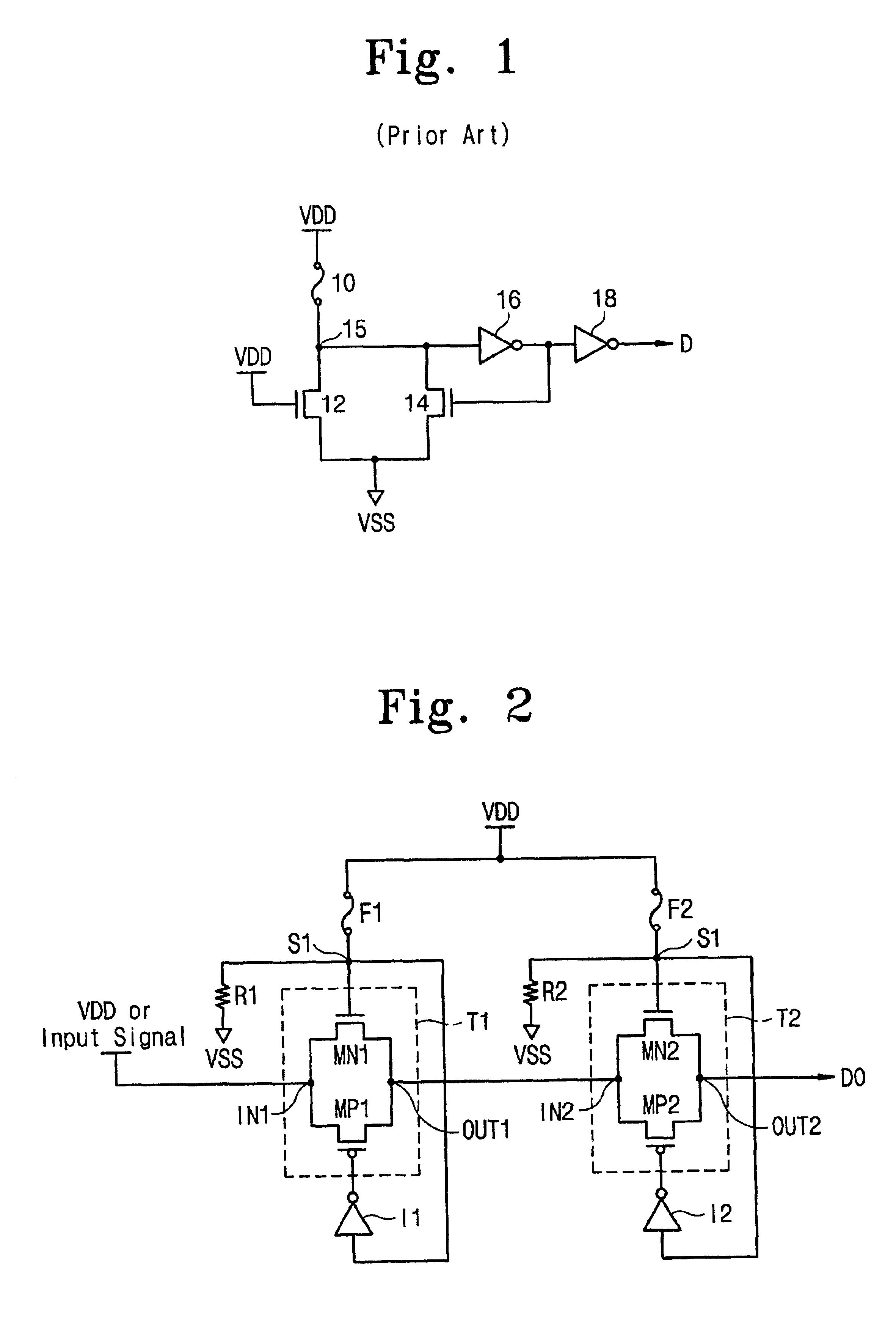
FIG. 2 is a circuit diagram of a fuse circuit according to an embodiment of the present invention

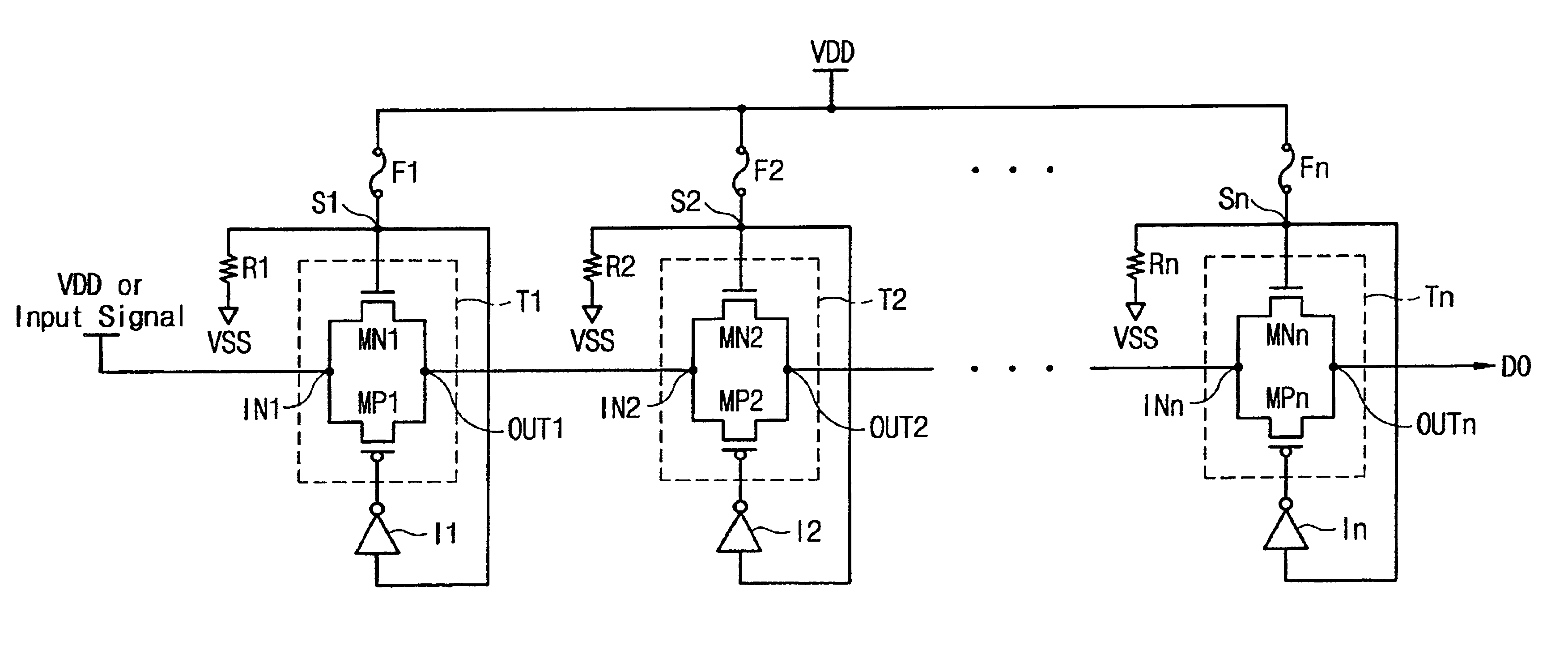
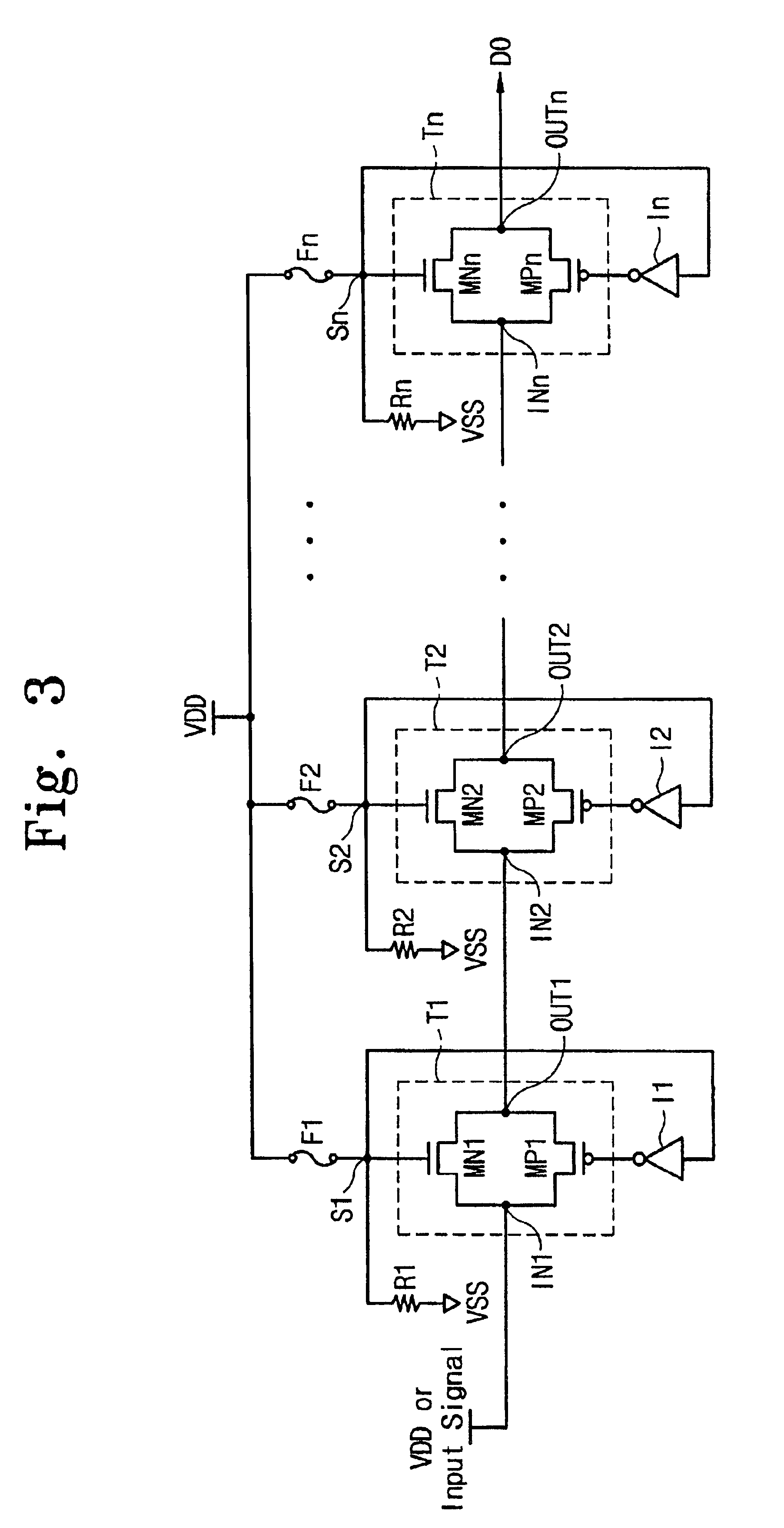
Referring to FIG. 2, the fuse circuit is formed of fuses F1 and F2, transmission gates T1 and T2, inverters I1 and I2, and resistors R1 and R2. The fuses F1 and F2 are made of polysilicon, or other metallic materials such as titanium (Ti) or titanium nitride (TiN) that can be cut out by a laser. Each of the fuses F1 and F2 is connected between power supply voltage VDD and sensing nodes S1 and S2. The transmission gate T1 is connected to the fuse F1, and inclu...


PUM


Abstract

In a fuse circuit including programmable fuses in a semiconductor integrated circuit, the fuses store specific information related to the semiconductor integrated circuit, such as redundancy information, wafer lot number, die lot number, and die position on the wafer, etc. The fuse circuit utilizes a plurality of fuses for storing identical bit information. Consequently, in the case where a fuse has not been cut out correctly, the fuse circuit can reduce programming defects, whereby defect generation rates are remarkably decreased.

Description

This application relies for priority upon Korean Patent Application No. 2000-61257, filed on Oct. 18, 2000, the contents of which are herein incorporated by reference in their entirety.FIELD OF THE INVENTIONThe present invention relates generally to semiconductor integrated circuit devices, and more particularly to a fuse circuit employed in a semiconductor integrated circuit.BACKGROUND OF THE INVENTIONAs the storage capacity of integrated circuit memories continues to increase through higher integration, associated memory cell defects rise accordingly, due to increased complexity in manufacturing processes, leading to degradation of production yield. In general, it is difficult to render a memory device having no defective cells. Therefore, various attempts have been made to improve the production yields of the highly integrated memory devices.It is preferable to improve the manufacturing process to suppress the generation of the defective cells; but there are limitations. Thus, ot...

Claims


Application Information

Patent Timeline
IPC IPC(8): G11C17/14G11C17/16G11C29/00
CPCG11C17/16G11C29/00
Inventor JUNG, CHANG-WHANKIM, EUN-HAN
Owner SAMSUNG ELECTRONICS CO LTD
Learn More