Chip welding apparatus and/or lead binding apparatus with chip hold-down device

A chip bonder and wire bonding technology, applied in welding/cutting auxiliary equipment, auxiliary devices, welding equipment, etc., can solve problems such as wear marks of matrix substrates

Inactive Publication Date: 2002-07-10
ESEC TRADING
View PDF0 Cites 2 Cited by
  • Summary
  • Abstract
  • Description
  • Claims
  • Application Information

AI Technical Summary

Problems solved by technology

During this transfer, undesired wear marks may be produced on the underside of the matrix substrate

Method used


Image

  • Chip welding apparatus and/or lead binding apparatus with chip hold-down device
  • Chip welding apparatus and/or lead binding apparatus with chip hold-down device
  • Chip welding apparatus and/or lead binding apparatus with chip hold-down device

Examples


Embodiment 1

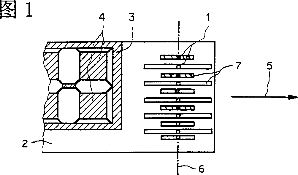
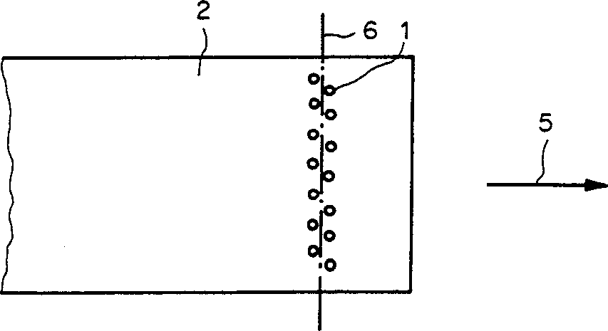
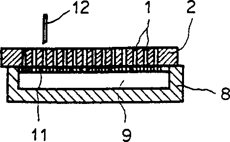
[0021] image 3 A cross-sectional view of the pressing device taken along line 6 in FIG. 1 is shown. The table 2 has a detachable drawer 8, the drawer 8 is combined with the bottom of the table 2, and a slot 9 is formed at the bottom of the drawer 8. During operation, the tank 9 is connected to a vacuum source. In addition, three cams 10 are arranged at the bottom of the drawer 8 (see Figure 4 ). The sheet 11 is inserted into the drawer 8 so that the cam 10 fits into the corresponding hole made in the sheet 11. For the sheet, it is preferable to use a rigid polyvinyl chloride (PVC) sheet such as that sold by VinK AG under the trade name VIKUNYL. The bore 1 of the table 2 is opened on the sheet 11 in the area of ​​the groove 9. When a new type of substrate is reconfigured for the die bonder, the drawer 8 is pulled out, the new slice 11 lubricated by vacuum lubricating oil replaces the slice 11 inserted into the drawer 8, and then the drawer 8 is pushed Into Taiwan 2. In this case...

Embodiment 2

[0024] Figure 5 , 6 The embodiment shown is not suitable for matrix substrates, but is suitable for substrates without notches such as BGA  Substrate. Figure 5 The table 2 shown in the top view has at least two cavities 20.1-20.6 with different lengths on the lower surface, and the cavities are connected to a continuous groove 19. In this embodiment, the number of cavities 20.1-20.6 is six. Similar to the first embodiment, this embodiment provides a drawer 8. Figure 6 The drawer 8 shown in has a surface 21 on which 6 cavities 22.1-22.6 are arranged. The cavities 22.1-22.6 have one lateral branch facing the groove 19 and two or three lateral branches facing the borehole 1. Before insertion, vacuum lubricant is applied to the surface 21. The surface 21 of the drawer 8 is placed on the lower surface of the table 2, so that the groove 19 forms a channel through which a vacuum can be applied. Vacuum lubricating oil can ensure that the channels and cavities 20.1-20.6 and cavities 22...


PUM


Abstract

A Die Bonder or a Wire Bonder contains a device for holding down a substrate. The device comprises a table with drill holes. The drill holes are mechanically programmable with regard to whether vacuum can be applied to them or not. The mechanical programming enables a fast and easy adaptation of the device to different substrates.

Description

Invention field [0001] The invention relates to a die bonder and / or wire bonder with a device for pressing a substrate. The type of the substrate is defined by the preamble of claim 1. Background of the invention [0002] When a semiconductor chip is mounted on a substrate using a so-called die bonder, in the conveying direction and / or in the transverse direction of the conveying direction, a predetermined number of cycles are transferred on the supporting surface by passing the substrate through several cycles. Distance, the semiconductor chip can be mounted in a predetermined position. The die bonder developed by the applicant is used to place the substrate on a rigidly arranged disk, which has a bore hole that can be connected to a vacuum source to suck and compress the substrate. For the processing of so-called matrix substrates, the chip areas on the substrate for receiving semiconductor chips are arranged in rows and columns, and it is difficult to apply a pressing device w...

Claims


Application Information

Patent Timeline
IPC IPC(8): H01L21/52B23K37/04
CPCH01L2924/0002B23K2201/40B23K37/0426B23K2101/40H01L2924/00H01L21/52
Inventor 施特凡·伯赫勒吕迪·格吕特雷托·舒比格罗尔夫·舒尔曼比特·聪比尔
Owner ESEC TRADING
Why Eureka
Try Eureka