Scintillation correction apparatus, scintillation correction method and recording medium for storing scintillation correction program

A correction device and correction value technology, which is applied to radiation control devices, parts of color TV, parts of TV system, etc., can solve problems such as long time

Inactive Publication Date: 2003-08-20
SHARP KK
View PDF1 Cites 26 Cited by
  • Summary
  • Abstract
  • Description
  • Claims
  • Application Information

AI Technical Summary

Problems solved by technology

Therefore, it takes a long time to perform flicker correction according to the frame or field frequency of an imaging device

Method used


Image

  • Scintillation correction apparatus, scintillation correction method and recording medium for storing scintillation correction program
  • Scintillation correction apparatus, scintillation correction method and recording medium for storing scintillation correction program
  • Scintillation correction apparatus, scintillation correction method and recording medium for storing scintillation correction program

Examples


example 1

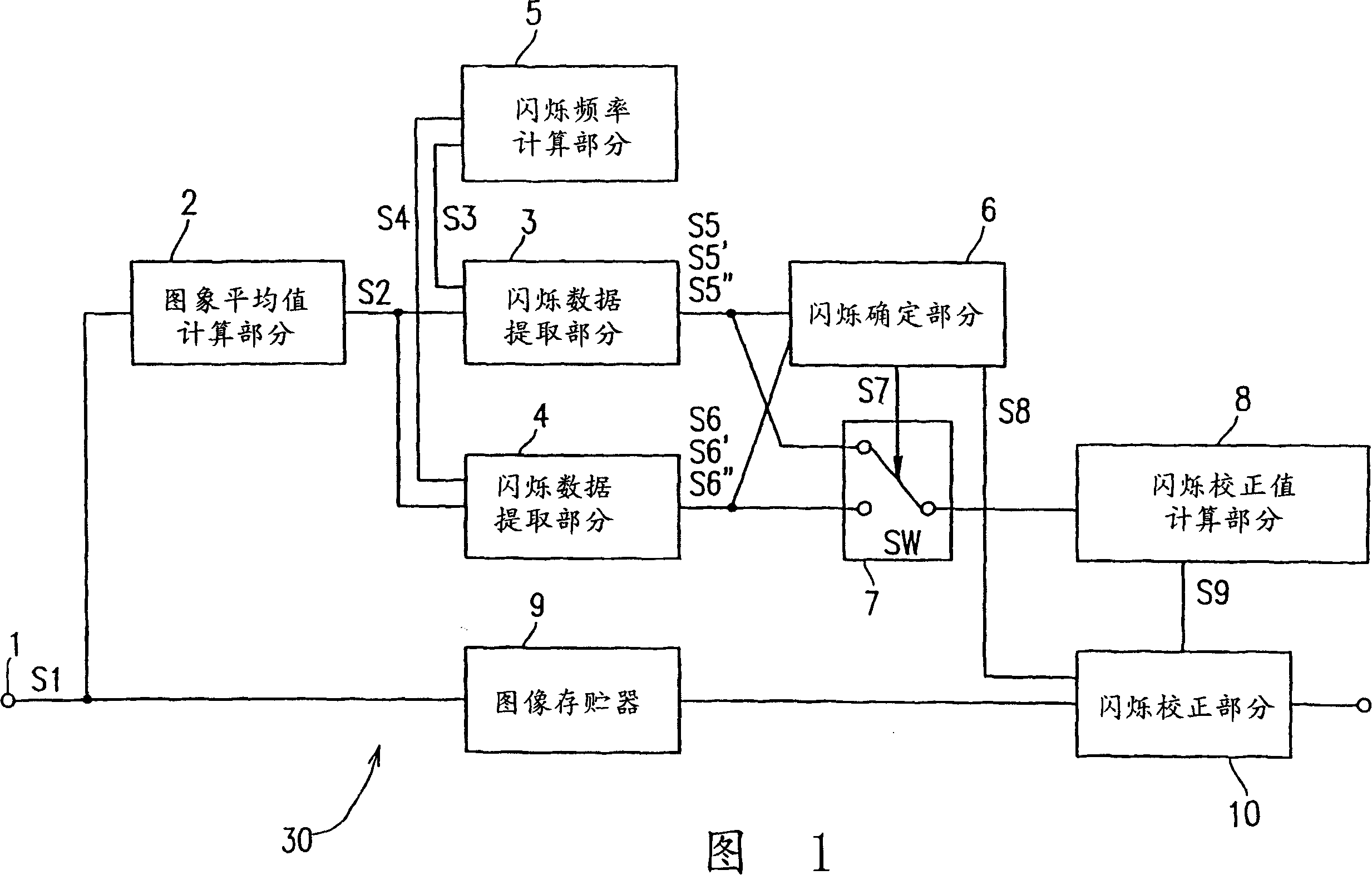
[0067] FIG. 1 is a schematic block diagram illustrating the structure of a flicker correcting device 30 according to a first example of the present invention.

[0068] This flicker correcting device 30 has an input port 1 through which an image signal S1 is input. The image signal S1 is obtained by imaging an object using a camera including an imaging device such as an electronic camera, a scanner or the like. For example, when an object is imaged with a video camera including an X-Y addressing scanning type solid-state imaging device (for example, a CMOS type image sensor, etc.), under the illumination of a fluorescent lamp that flickers in synchronization with the frequency of the AC power supply , the image signal S1 including the flicker component is input through the input port 1 .

[0069] The image S1 input through the input port 1 is sent to an image memory 9, and one frame or one field of the image signal is stored in the image memory 9 as image data. The image sign...

example 2

[0099] Figure 4 is a schematic block diagram illustrating the structure of the flicker correcting device 40 according to the second example of the present invention.

[0100] This flicker correcting device 40 is not provided with the image memory 9 like in the flicker correcting device 30 of Example 1 (FIG. 1). For example, a flicker correction value is calculated based on a frame or field of an image signal input through an input port 1, such as a first previous frame or field, and this flicker correction value is used to correct the current input through the input port 1. A frame or field of an image signal. In this case, there is a phase difference of the flicker component between the previous frame (or field) and the current frame (or field), whereby flicker correction is achieved by referring to the phase difference. The flicker correction device 40 in Example 2 has a phase difference calculation section 11 in order to calculate the phase difference.

[0101] As with ...

example 3

[0112] Figure 5 is a schematic block diagram illustrating the structure of a flicker correcting device 50 according to the third example of the present invention.

[0113] In this flicker correcting device 50, an image signal S1 input from the input port 1 is sent to the image average calculation section 2 and the flicker correcting section 10, as in the flicker correcting device 40 of Example 2 ( Figure 4 ). In addition, the image signal S1 is sent to the flicker correction value calculation section 8 .

[0114] Since the contrast is reduced in the dark part, the horizontal alternating light and dark striped pattern caused by the flicker phenomenon is more prominent in the light part than in the dark part. Therefore, when a bright pixel and a dark pixel appear If the same flicker correction value is added to bright pixels and dark pixels on the same horizontal line in the frame or field of the image, the image quality will be degraded.

[0115] In order to avoid such deg...


PUM


Abstract

A flicker correction apparatus for correcting a flicker component of an image signal obtained by imaging an object using an imaging device is provided. The apparatus comprises an image average calculation section for calculating an average of the image signal, a flicker frequency calculation section for calculating a flicker frequency, a flicker data extraction section for extracting flicker data using the average of the image signal and the flicker frequency, a flicker determination section for determining the presence or absence of a flicker phenomenon using the flicker data, a flicker correction amount calculation section for calculating a flicker correction amount using the flicker data, and a flicker correction section for removing the flicker component of the image data using the flicker correction amount.

Description

technical field [0001] The present invention relates to a flicker correction device, a flicker correction method, and a recording medium storing a flicker correction program for correcting a flicker component of an image signal obtained by imaging an object with an imaging device . More specifically, the present invention relates to a flicker correction device, a flicker correction method, and a recording medium storing a flicker correction program capable of preventing the flicker phenomenon from occurring. The flicker phenomenon refers to that when an X-Y addressing scanning solid-state imaging device is used to image an object under the illumination of a fluorescent lamp, and the fluorescent lamp flickers synchronously with the frequency of the alternating current (AC) power supply, the horizontal direction appears in the image. A striped pattern of stretched dark sections alternating with light sections. Background technique [0002] Electronic cameras, such as video c...

Claims


Application Information

Patent Timeline
Patent Type & Authority Applications(China)
IPC IPC(8): H01L27/146H04N5/235H04N5/335H04N5/351H04N5/357H04N5/374H04N5/378
CPCH04N5/2357H04N5/235Y10S348/91H04N23/70H04N23/745H04N5/21
Inventor 吉田卓司木村胜治久保登奥畑宏之加谷俊之滨中慎介小野荣滋白川功
Owner SHARP KK
Why Eureka
Try Eureka