
Photoelectric device and electronic equipment

An electro-optic device and electro-optic technology, applied in optics, nonlinear optics, instruments, etc., can solve the problems of columnar pads that cannot achieve resistance, cannot be eliminated, and match, and achieve the goal of reducing display unevenness and improving quality Effect

Inactive Publication Date: 2003-09-10
BOE TECH GRP CO LTD
View PDF1 Cites 8 Cited by
  • Summary
  • Abstract
  • Description
  • Claims
  • Application Information

AI Technical Summary

Problems solved by technology

Because, in the pasting process, as described above, since the two substrates are pasted together with an appropriate pressure, although the result is that the above-mentioned sealant or the gap member in the sealant are opposed to each other as if they resist the pressure. The approaching substrate produces a prescribed resistance, but there is no such sealant and gap member on the portion where the liquid crystal injection port exists.
[0012] Here, even if it is assumed that there are columnar spacers as the above-mentioned spacers between the two substrates, it is impossible to eliminate the above-mentioned disadvantages.
Because, due to the relatively high pressure in the above-mentioned pasting process, the resistance produced by the columnar spacer has not yet reached the level that can match the resistance produced by the above-mentioned sealant and gap members.

Method used


Image

  • Photoelectric device and electronic equipment
  • Photoelectric device and electronic equipment
  • Photoelectric device and electronic equipment

Examples


Embodiment Construction

[0103] Hereinafter, embodiments of the present invention will be described with reference to the drawings. The following embodiments are embodiments in which the electro-optical device of the present invention is applied to a liquid crystal display device.

[0104] The overall composition of the electro-optical device

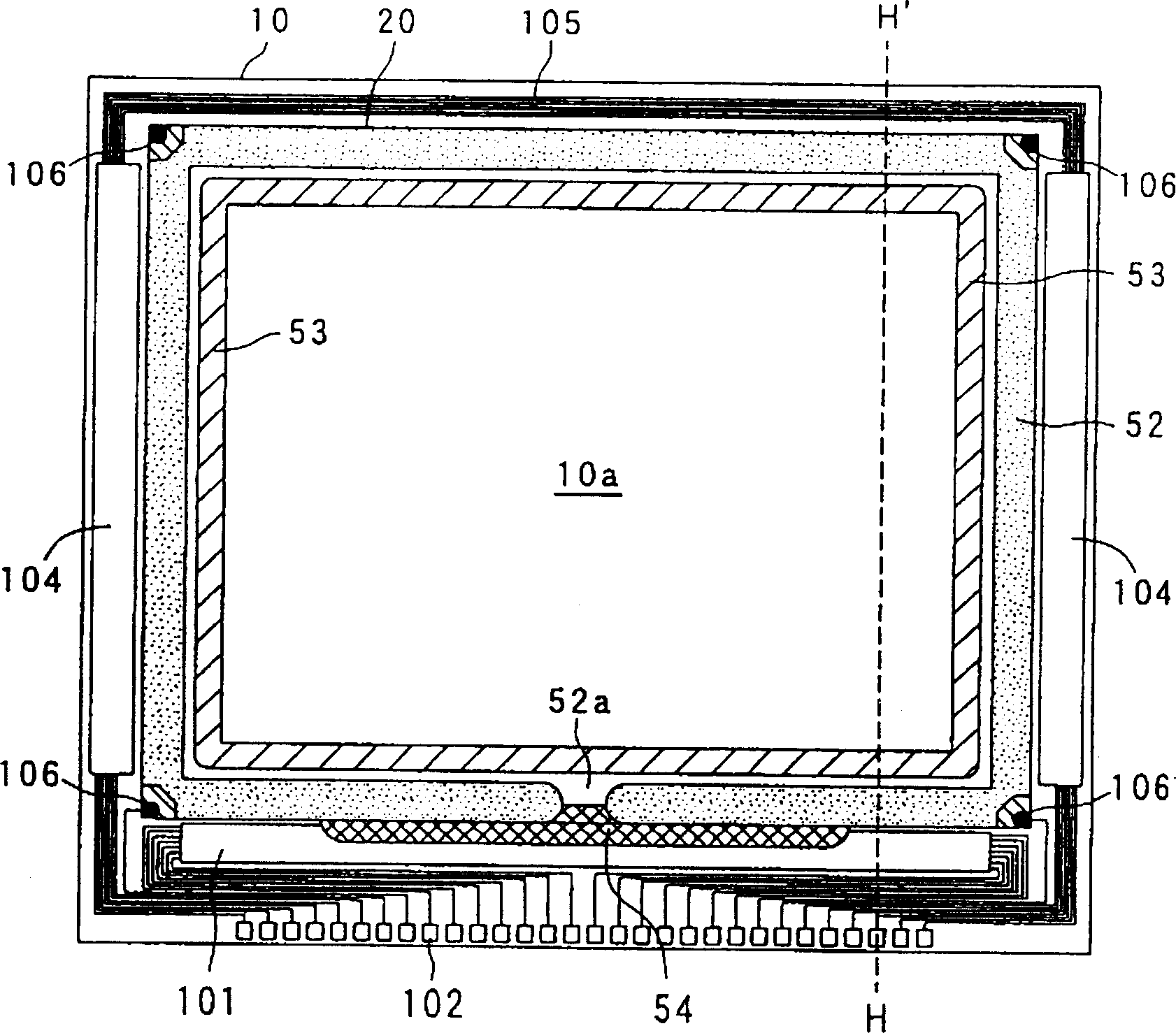
[0105] First, see figure 1 and figure 2 The overall configuration of the electro-optical device of this embodiment will be described. in addition, figure 1 It is a plan view of the TFT array substrate viewed from the counter substrate 20 side together with each constituent element formed thereon, figure 2 yes figure 1 The H-H' profile.

[0106] exist figure 1 and figure 2 In the electro-optical device of this embodiment, the TFT array substrate 10 and the counter electrode 20 are arranged to face each other. Between the TFT array substrate 10 and the opposite substrate 20, a liquid crystal layer 50 has been sealed, and the TFT array substrate 10 and...


PUM


Abstract

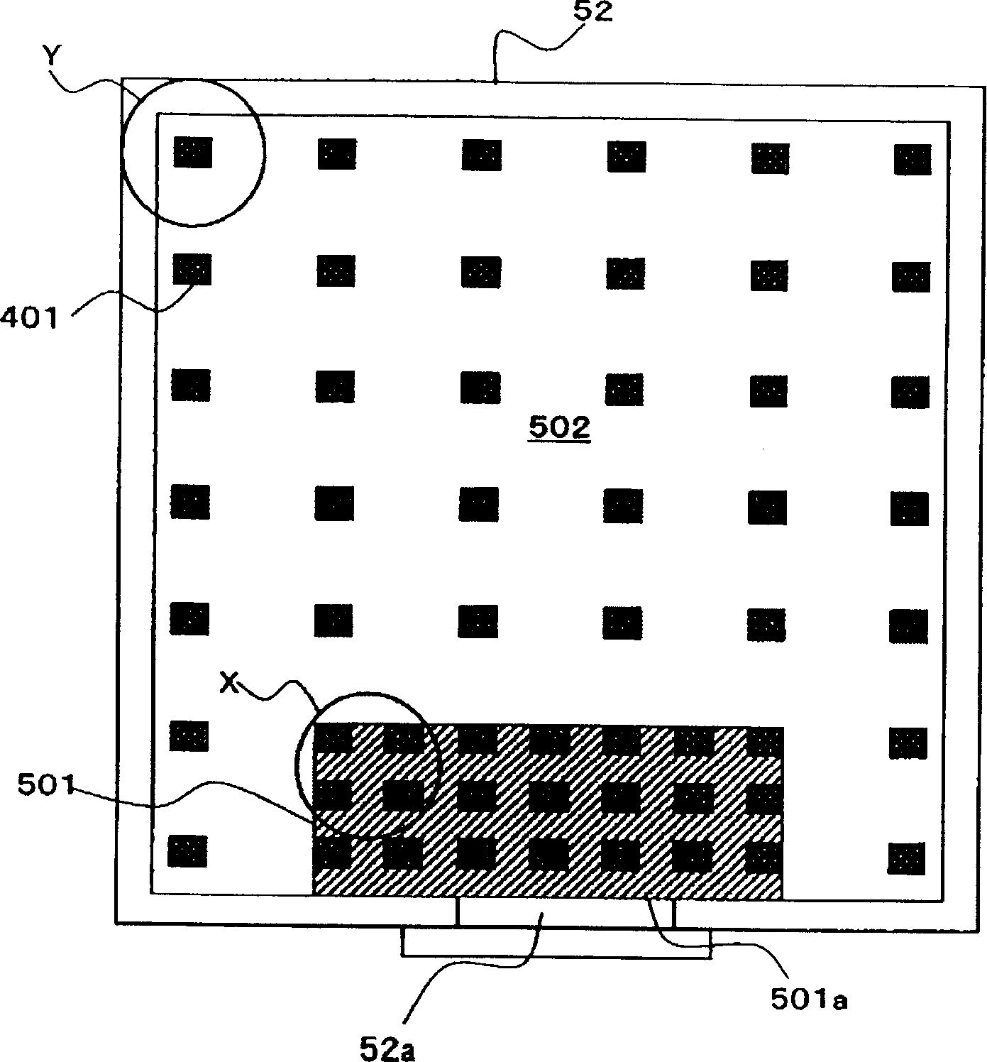
The invention provides an electro-optic device capable of keeping the cell gap constant or substantially constant throughout the substrate surface regardless of the existence of a liquid crystal inlet. The electro-optic device of the invention has a TFT array substrate and an opposite substrate formed to sandwich an electro-optic material; a liquid crystal inlet to communicate the clearance sandwiched between the substrates with the exterior; and a plurality of columnar spacers scattered within the surfaces in parallel to the substrates to keep the clearance between the substrates at a predetermined thickness, the columnar spacers being disposed more densely in the vicinity of the liquid crystal inlet and more sparsely in the other area within the surfaces.

Description

technical field [0001] The present invention belongs to the technical field of electro-optic devices and electronic equipment, and in particular, belongs to an electro-optic device using a columnar spacer and an electronic device comprising such an electro-optic device in order to keep the gap between two substrates at a predetermined value. equipment. Background technique [0002] Electro-optical devices such as liquid crystal display devices are generally constructed by sealing liquid crystal between two substrates on which upper electrodes, wiring, elements, etc. have been formed. In such an electro-optic device, in order to keep the gap between the two substrates at a constant (for example, about 3 to 5 micrometers) between the two substrates, that is, to keep the liquid crystal composed of liquid crystal constantly The thickness of the layer (hereinafter referred to as "cell gap") generally requires a so-called spacer to be provided on the entire surface of the substra...

Claims


Application Information

Patent Timeline
IPC IPC(8): G02F1/1339G02F1/1341
CPCG02F1/13394G02F1/1341G02F1/1339
Inventor 安达勲
Owner BOE TECH GRP CO LTD
Learn More