Method and system for manufacturing liquid crystal display device

a technology of liquid crystal display and manufacturing method, which is applied in the direction of instruments, other domestic objects, chemistry apparatus and processes, etc., can solve the problems of liquid crystal panel distorted, suppress panel distortion, reduce display unevenness of liquid crystal panel, and reduce interference with bezel and interferen

Inactive Publication Date: 2012-11-22
NITTO DENKO CORP
View PDF4 Cites 10 Cited by
  • Summary
  • Abstract
  • Description
  • Claims
  • Application Information

AI Technical Summary

Benefits of technology

[0009]Therefore, if the warping direction can be controlled in the roll bonding process where a liquid crystal panel is more likely to be warped, it will be very advantageous in manufacture. It is therefore an object of the invention, which has been accomplished in view of the above circumstances, to provide liquid crystal display device manufacturing method and system that can control the direction of warping of a liquid crystal panel as desired.
[0012]This process makes it possible to warp the liquid crystal panel toward the back side, so that the interference between the liquid crystal panel and a bezel or a backlight unit can be reduced, which makes it possible to suppress panel distortion and to reduce display unevenness of the liquid crystal panel.
[0015]The pressure-sensitive adhesive should have a storage modulus of 1.0×10⁴ to 5.0×10⁴ [GPa], which is an indicator of the ability of the pressure-sensitive adhesive to relax stress.
[0018]This feature is preferred because it can increase the warping toward the back side.
[0021]According to this feature, a pair of the optical films bonded in the same direction can act to cancel the stresses together, so that the liquid crystal panel is warped by the stress on the optical film bonded in the final direction where the stress finally remains without being cancelled (see for example FIG. 5). In a preferred mode, therefore, the optical film is bonded finally to the back side so that stress can remain on the back side without being cancelled. This feature is preferred because the warping can be cancelled out in the liquid crystal panel, so that the warping after the cancellation is not significant and the total amount of warping can be controlled to be small.
[0026]This system can warp the liquid crystal panel toward the back side, so that it can reduce interference with a bezel and interference with a backlight unit, suppress panel distortion, and reduce display unevenness of the liquid crystal panel.

Problems solved by technology

If a warped liquid crystal panel is incorporated into a liquid crystal TV module, it may interfere with a backlight unit, or stress may be applied from a bezel (outer frame), so that the liquid crystal panel may be distorted.
This may alter the cell gap of the liquid crystal panel to cause unevenness (see FIG. 7).
It will be obvious that warping toward the back side should be restricted, although it is effective, because over-warping will cause a problem such as interference with a bezel regardless of whether the warping is toward the viewer side or the back side.

Method used


Image

  • Method and system for manufacturing liquid crystal display device
  • Method and system for manufacturing liquid crystal display device
  • Method and system for manufacturing liquid crystal display device

Examples


embodiment 1

Method for Manufacturing Liquid Crystal Display Device

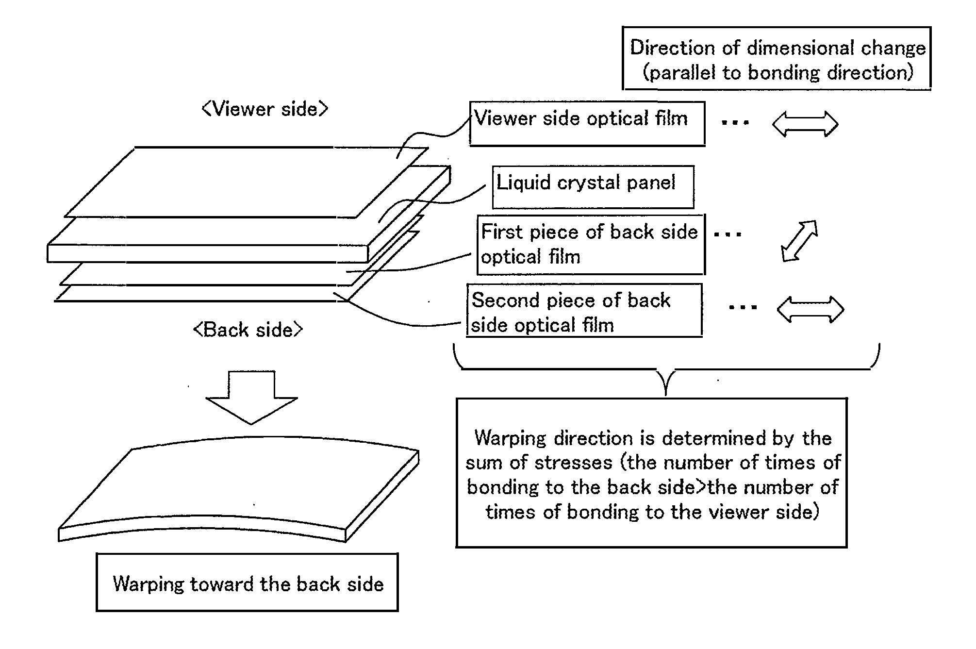
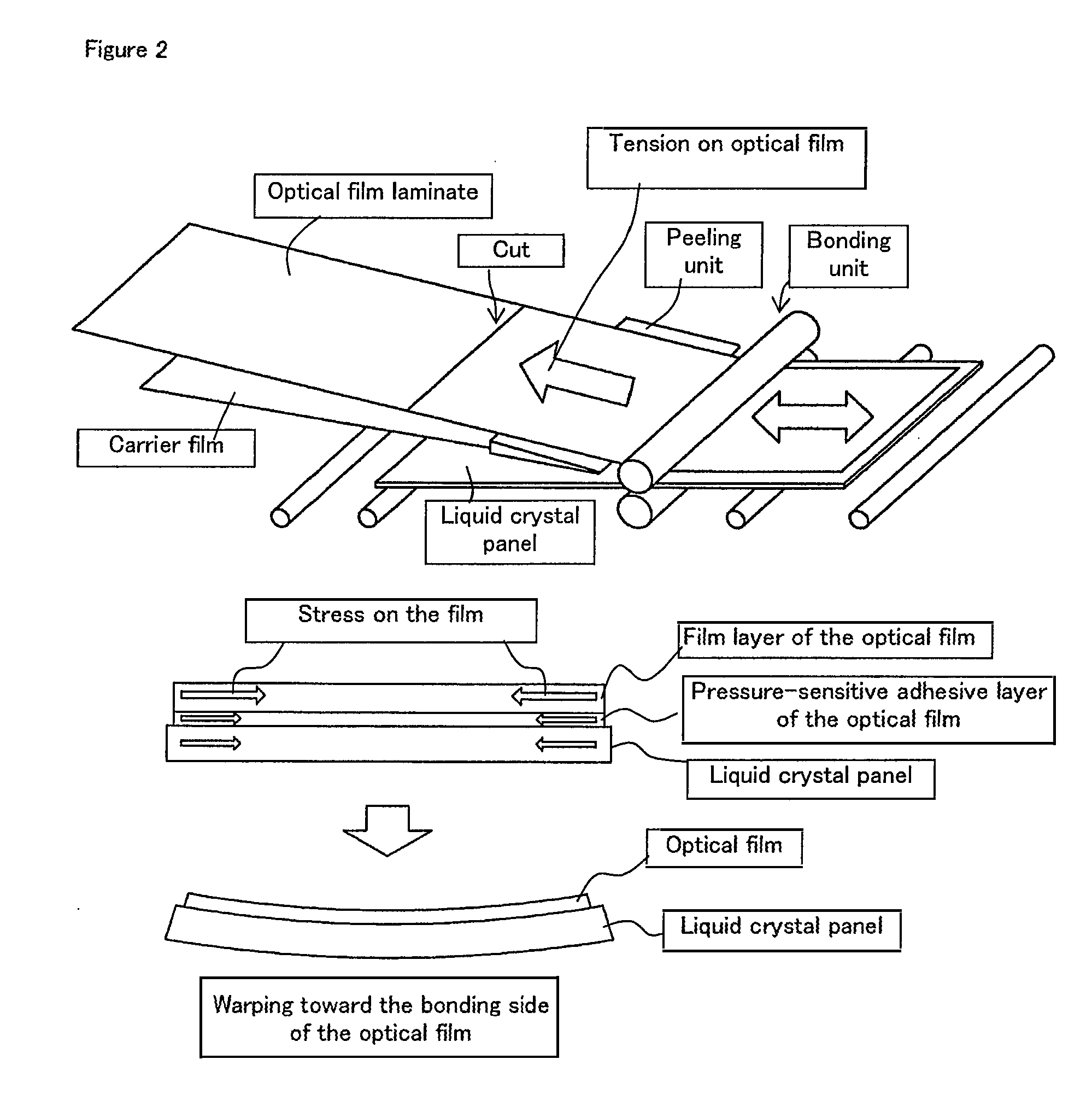
[0045]The liquid crystal display device manufacturing method includes: carrier film feeding steps including feeding long carrier films from continuous rolls, respectively, wherein the continuous rolls include rolls of laminates including the long carrier films and pressure-sensitive adhesive-carrying optical films each with a specific width placed on the carrier films, respectively; peeling steps including folding back each of the carrier films at a front end part placed on a carrier film feed path so that the optical films are peeled off from the carrier films, respectively; and bonding steps including bonding the optical films, which are peeled off or being peeled off in the peeling steps, to the viewer side and back side of a liquid crystal panel, wherein in the bonding steps, the optical films are bonded to the liquid crystal panel in such a manner that the number of times the optical film is bonded to the back side of the li...

examples

[0069]Different optical films were bonded to a liquid crystal panel (40 inch size) using the manufacturing system shown in FIG. 4. The manufacturing system was configured to perform the turnover and 90° rotation of the liquid crystal panel appropriately depending on the optical film type and the bonding order. When long optical films are cut into sheet pieces, the sizes of the sheet pieces are determined depending on the bonding side and the bonding direction.

[0070]The optical films used were a MD polarizing film (VEGQ1724DU manufactured by NITTO DENKO CORPORATION), a retardation film (ZEONOR Film manufactured by ZEON CORPORATION), and a reflective polarizing film (DBEF manufactured by 3M Company). In each example and comparative example, conditions were set up for the optical films, the bonding side of the liquid crystal panel (the back side or the viewer side), and the bonding direction (the direction of the long or short side), and evaluations were made of the direction and amoun...


PUM

PropertyMeasurementUnit
storage modulusaaaaaaaaaa
thicknessaaaaaaaaaa
temperatureaaaaaaaaaa

Abstract

The method for manufacturing a liquid crystal display device includes carrier film feeding steps including feeding long carrier films from continuous rolls, respectively; peeling steps including folding back each of the carrier films at a front end part placed on a carrier film feed path so that the optical films are peeled off from the carrier films, respectively; and bonding steps including bonding the optical films to the viewer side and back side of a liquid crystal panel, wherein in the bonding steps, the optical films are bonded to the liquid crystal panel in such a manner that the number of times the optical film is bonded to the back side of the liquid crystal panel is greater than the number of times the optical film is bonded to the viewer side of the liquid crystal panel.

Description

BACKGROUND OF THE INVENTION[0001]1. Field of the Invention[0002]The invention relates to a method and a system for manufacturing a liquid crystal display device.[0003]2. Description of the Related Art[0004]A conventional process of placing optical films on a liquid crystal panel includes cutting an optical film into a piece and bonding the piece of the optical film (sheet piece) to the liquid crystal panel. In such a bonding process, the tension on the optical film is very low and stable, and therefore, after the bonding, the liquid crystal panel is less likely to be warped due to variations in tension or over-tension. In recent years, an apparatus for simultaneously bonding pieces of optical films to both sides of a liquid crystal panel has been developed, which makes it easy to form uniform bonding states for the front and back sides during the bonding.[0005]On the other hand, it is known that there is a process including feeding a long carrier film from a continuous roll, wherein...

Claims


Application Information

Patent Timeline
Patent Type & Authority Applications(United States)
IPC IPC(8): B32B37/14B32B38/10
CPCB32B37/0015B32B37/02B32B37/185Y10T156/1195G02F1/1303G02F1/133536Y10T156/17B32B2457/202
Inventor HADA, KAZUYAHIRATA, SATOSHIKONDO, SEIJIUMEMOTO, SEIJI
Owner NITTO DENKO CORP
Why Eureka
Try Eureka