Photo transmitting device

An optical transmission and light source technology, applied in optics, nonlinear optics, time-division optical multiplexing systems, etc., can solve problems such as increased loss, increased cost, and difficulty in miniaturization, and achieve the effect of reducing optical loss

Inactive Publication Date: 2003-09-17
NIPPON TELEGRAPH & TELEPHONE CORP
View PDF4 Cites 4 Cited by
  • Summary
  • Abstract
  • Description
  • Claims
  • Application Information

AI Technical Summary

Problems solved by technology

In an ultra-high-speed optical transmission system, an LN (lithiun niobate) modulator that reduces the spectral width by modulation is used, but it is difficult to miniaturize, and using two sets requires a lot of installation space and increases the cost
Also, when two units are connected in parallel, the loss doubles
In addition, in optical transmission equipment that generates high-speed RZ codes and CS-RZ codes using optical time division multiplexing, two optical modulators are required for each channel, and there are problems similar to those described above.

Method used


Image

  • Photo transmitting device
  • Photo transmitting device
  • Photo transmitting device

Examples


Embodiment 1

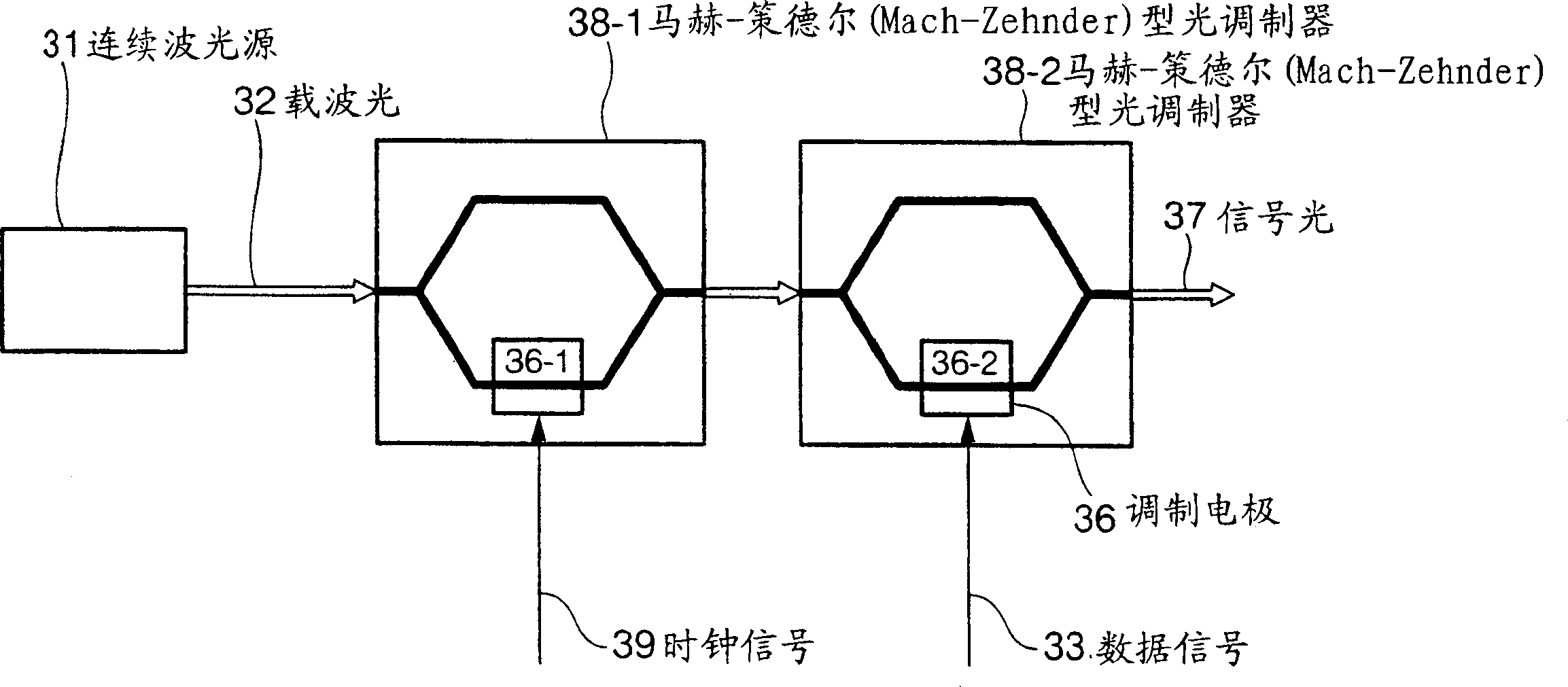
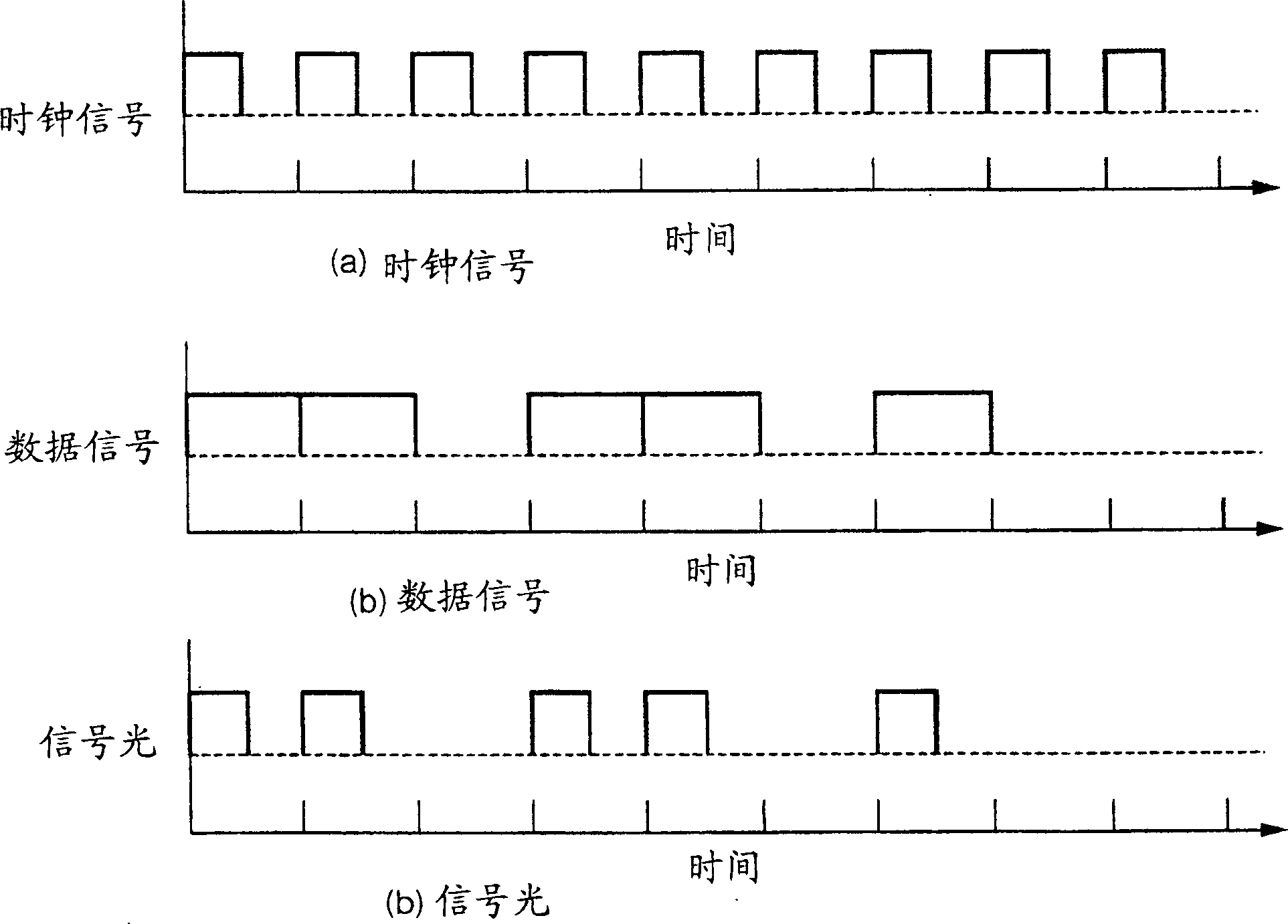
[0083] Figure 7An embodiment of the invention according to claim 1 is shown. The optical sending device includes: a continuous wave light source 11 outputting carrier light; a Mach-Zehnder optical modulator 18 with N (N is an integer greater than 2) modulation electrodes 16-1 to 16-N; The data signal is transformed into N return-to-zero transformation circuits 14-1~14-N of RZ encoding; the delay circuits 15-1~15-( N-1); As a component that provides a half-wavelength phase difference between the same arms to the input light of the interferometric light modulator, a bias of Vπ is applied to the arm of one side of the Mach-Zehnder type light modulator 18 Set circuit 10. Here, A is the frequency (Hz) of the signal velocity of the signal light 17, k is an integer from 1 to N-1, and Vπ is a driving voltage for shifting the phase of the input light by half a wavelength. Here, the bias circuit 10 is arranged on the arm on which the data signal is modulated, but it may also be arra...

Embodiment 2

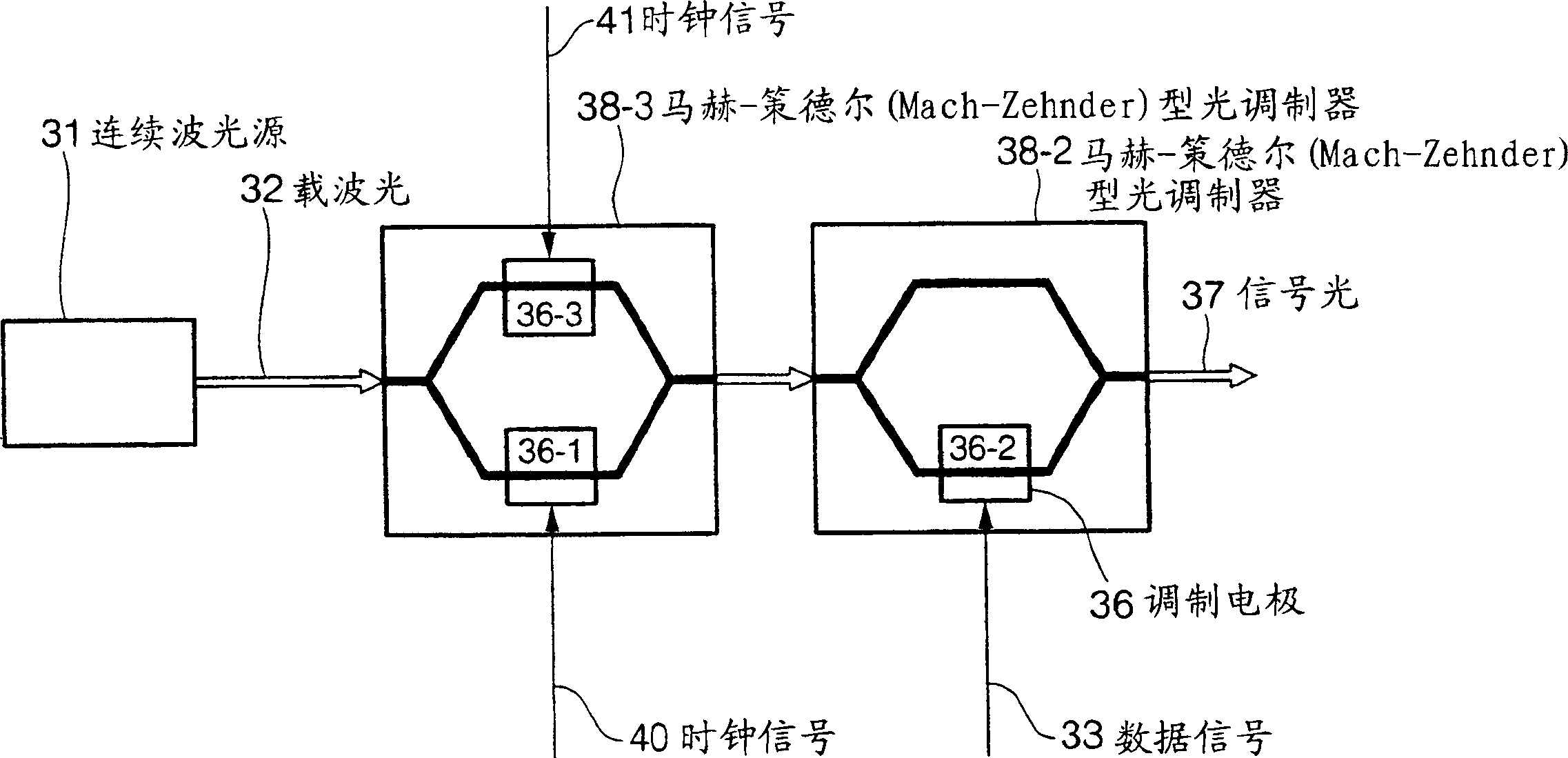
[0091] Figure 12 An embodiment of the invention according to claim 2 is shown. The optical sending device includes: a continuous wave light source 11 outputting carrier light; a Mach-Zehnder optical modulator 18 with N (N is an even number above 2) modulation electrodes 16-1 to 16-N; The data signal is transformed into N return-to-zero transformation circuits 14-1~14-N of RZ encoding; the delay circuits 15-1~15-( N-1); a signal polarity inversion circuit 19 for inverting the polarity of the even-numbered data signal. Here, A is the frequency (Hz) of the signal velocity of the signal light 17, and k is an integer from 1 to N-1. Here, the signal polarity inversion circuit 19 is arranged for even-numbered data signals, but may be arranged for odd-numbered data signals. The connection order of the signal polarity inversion circuit 19, the delay circuit 15, and the return-to-zero conversion circuit 14 can be interchanged.

[0092] Carrier light 12 from a continuous wave light ...

Embodiment 3

[0097] FIG. 15 shows an embodiment of the invention according to claim 3 . This optical transmission device comprises: a pulse light source 21 outputting pulsed light; a Mach-Zehnder type optical modulator 18 with N (N is an even number above 2) modulation electrodes 16-1 to 16-N; the data coded by NRZ The signal is converted into N return-to-zero conversion circuits 14-1~14-N of RZ code; the delay circuits 15-1~15-(N -1); a signal polarity inversion circuit 19 for inverting the polarity of the even-numbered data signal. Here, A is the frequency (Hz) of the signal velocity of the signal light 17, and k is an integer from 1 to N-1. Here, the signal polarity inversion circuit 19 is arranged for even-numbered data signals, but may be arranged for odd-numbered data signals. The connection order of the signal polarity inversion circuit 19, the delay circuit 15, and the return-to-zero conversion circuit 14 can be interchanged.

[0098] The pulsed light 26 from the pulsed light so...


PUM


Abstract

The present invention relates to optical transmission devices. The optical transmission device of the present invention is an optical transmission device that multiplexes a plurality of input electrical signals into an optical signal at a signal speed of frequency A, and includes: a light source that provides carrier light; and distributes the carrier light from the light source into N ( An optical distribution circuit where N is an integer); an optical modulator for modulating the carrier light distributed by the distribution circuit with electrical signals; an optical coupling circuit for synthesizing the optical signals from the optical modulator; converting the above-mentioned input electrical signals into The RZ encoding of the pulse width below 1 / A is sequentially supplied to the components input to the above-mentioned optical modulator after each staggered delay time of 1 / A.

Description

technical field [0001] The present invention relates to an optical transmission device that multiplexes a plurality of electrical signals, converts them into optical signals, and transmits them. [0002] This application is based on Japanese Patent Application No. 2002-059632, No. 2002-230457, which are incorporated herein by reference. Background technique [0003] Since the frequency utilization efficiency can be easily improved, as a method of increasing the capacity of the optical transmission line, the speed of each wavelength is being increased. In order to keep the transmission distance constant and increase the speed, high input light intensity is required. However, in high-speed optical transmission, the degradation of transmission quality due to various factors such as signal-to-noise ratio degradation, nonlinear optical effects, group velocity dispersion, and polarization mode dispersion has become a serious problem. Therefore, it is desired to replace NRZ (non-r...

Claims


Application Information

Patent Timeline
Patent Type & Authority Applications(China)
IPC IPC(8): G02F1/03G02F1/035H04B10/516H04B10/524H04B10/588H04B10/61H04J3/00H04J14/08
CPCH04J14/08
Inventor 木坂由明富泽将人平野章
Owner NIPPON TELEGRAPH & TELEPHONE CORP
Why Eureka
Try Eureka