Optical element, optical element chip, and corresponding producing method

A technology for optical elements and manufacturing methods, which is applied in the manufacture of optical elements, optical heads, recording/reproducing by optical methods, etc., and can solve problems such as peeling of optical films

Inactive Publication Date: 2004-01-21
TOMOEGAWA PAPER CO LTD
View PDF2 Cites 0 Cited by
  • Summary
  • Abstract
  • Description
  • Claims
  • Application Information

AI Technical Summary

Problems solved by technology

During the thermal cycle test after the electronic device is manufactured, the air between the cover and the optical film will expand, and there is a risk that the optical film will be peeled off from the cover

Method used


Image

  • Optical element, optical element chip, and corresponding producing method
  • Optical element, optical element chip, and corresponding producing method
  • Optical element, optical element chip, and corresponding producing method

Examples


Embodiment Construction

[0035] Hereinafter, the present invention will be described in detail.

[0036] (Optical element)

[0037] The optical element of the present invention is an element in which an optical film is attached to a substrate, and is characterized in that the optical film is only partially formed.

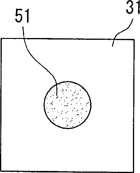
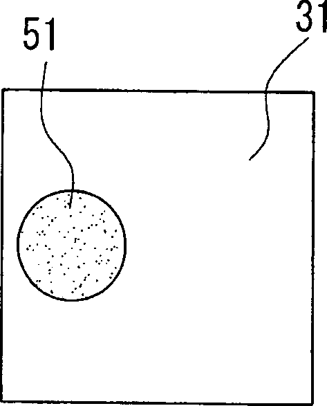
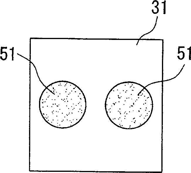
[0038] As a specific configuration example of the optical element of the present invention, as shown in FIG. The sticking position of the optical film 51 on the base 31 is not limited to the central portion of the base 31 , as shown in FIG. 1( b ), the optical film 51 may be attached to the end of the base 31 . As shown in FIG. 1( c ), it is also possible to form a structure in which a plurality of optical films 51 are attached.

[0039] As other configuration example shown in Fig. 1 (d) and (e), can enumerate following configuration: place all sticks optical film 51 except the four jiaos of substrate 31, as shown in Fig. 1 (f), An optical film is attached to all but one corner of the b...


PUM


Abstract

Provided is an optical element wafer on which a plurality of optical elements are formed altogether, whose cost can be reduced and in which an optical film is prevented from partly peeling and floating when stuck to a package main body. The optical element wafer 10 comprises a base material preform 30, and a holding material 40 stuck to one of the sides of the base material preform 30. The base material preform 30 has a plurality of base materials 31 formed by dividing the base material preform 30. The optical film 51 is partially stuck to each base material 31.

Description

technical field [0001] The present invention relates to an optical element bonded to a housing body for accommodating electronic components, an optical element wafer capable of manufacturing, storing, and transporting a plurality of optical elements in batches, and a corresponding manufacturing method. Background technique [0002] Conventionally, after accommodating various electronic components in a box-shaped case main body having an opening, a cover for sealing the electronic device (hereinafter, sometimes simply referred to as a "cover") is connected to the opening side end of the case main body. Part bonding, electronic components are accommodated in the case composed of the case body and the cover, and various electronic devices are manufactured. Such an electronic device is used, for example, as a device for an optical pickup or the like. [0003] In recent years, for devices for optical pickups, for example, it has been proposed to attach a retardation film as an o...

Claims


Application Information

Patent Timeline
Patent Type & Authority Applications(China)
IPC IPC(8): G02B3/00B32B3/00G11B7/12G11B7/123G11B7/1365G11B7/22
CPCH01L27/14625H01L27/14685G11B7/1365B32B3/00G11B7/123G11B7/22Y10T428/24802G02B5/30
Inventor 手塚明相川文则土田雅之驹形文规
Owner TOMOEGAWA PAPER CO LTD
Why Eureka
Try Eureka