Schotthy barrier transistor and manufacturing method thereof

A technology of Schottky potential and transistors, which is applied in the direction of transistors, semiconductor/solid-state device manufacturing, semiconductor devices, etc., can solve problems such as the inability to use metal gates, the soft error rate of the junction interface, and the high floating body effect, so as to reduce etching damage effect

Inactive Publication Date: 2004-10-20
ELECTRONICS & TELECOMM RES INST
View PDF1 Cites 22 Cited by
  • Summary
  • Abstract
  • Description
  • Claims
  • Application Information

AI Technical Summary

Problems solved by technology

Therefore, metal gates cannot be used
Fourth, the soft error rate (soft error) of the junction interface is high and produces a floating body effect (floating body effect)
So far, there is no effective solution to etch damage

Method used


Image

  • Schotthy barrier transistor and manufacturing method thereof
  • Schotthy barrier transistor and manufacturing method thereof
  • Schotthy barrier transistor and manufacturing method thereof

Examples


Embodiment Construction

[0018] The present invention will now be described more fully with reference to the accompanying drawings, in which preferred embodiments of the invention are shown. However, the present invention can be embodied in many different forms and is not limited to the embodiments set forth herein. Rather, these embodiments are provided so that this disclosure will be thorough and complete, and will fully convey the scope of the invention to those skilled in the art. In the drawings, the form of elements is exaggerated for clarity. To facilitate understanding, identical reference numerals have been used wherever possible to denote identical elements in the drawings.

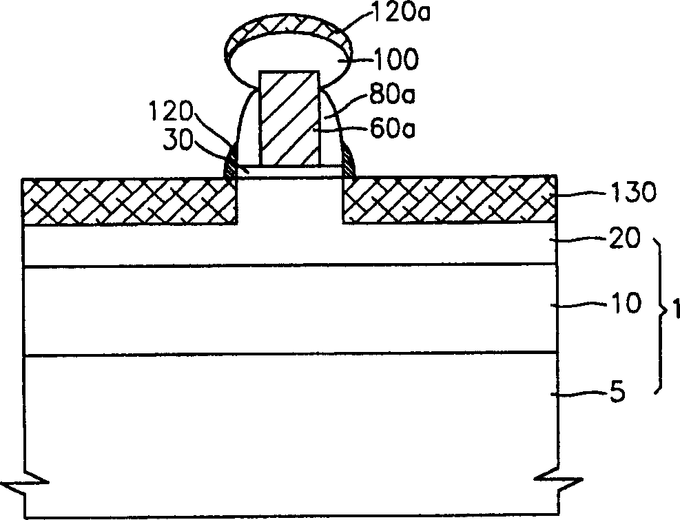
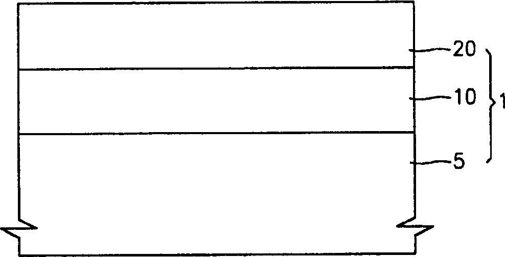
[0019] figure 1 is a cross-sectional view of an SB transistor according to one embodiment of the present invention. refer to figure 1 , the entire structure is formed on a silicon-on-insulator (SOI) wafer 1 . The SOI wafer 1 has a sequentially stacked structure of a base silicon layer 5 , a buried oxide layer 10 as...


PUM


Abstract

A schottky barrier transistor and a method of manufacturing the same are provided. The method includes forming a gate insulating layer and a gate on a substrate, forming a spacer on a sidewall of the gate, and growing a polycrystalline silicon layer and a monocrystalline silicon layer on the gate and the substrate, respectively, using a selective silicon growth. A metal is deposited on the polycrystalline silicon layer and the monocrystalline silicon layer. Then, the metal reacts with silicon of the polycrystalline silicon layer and the monocyrstalline silicon layer to form a self-aligned metal silicide layer. Therefore, selective wet etching for removing an unreacted metal after silicidation can be omitted. Furthermore, etching damage caused during the formation of the spacer can be decreased during the growth of the monocrystalline silicon layer, thereby improving the electrical characteristics of devices.

Description

[0001] This application claims priority from Korean Patent Application No. 2003-23969 filed in the Korean Intellectual Property Office on April 16, 2003, the entire disclosure of which is incorporated herein by reference. technical field [0002] The invention relates to a transistor and its manufacturing method. More particularly, the present invention relates to a Schottky barrier transistor (hereinafter referred to as "SB" transistor) using a schottky barrier formed between a metal and a semiconductor, and a method of manufacturing the same. Background technique [0003] At present, semiconductor device manufacturing technology has reached the level of being able to manufacture transistors with short channel lengths less than 100nm. However, achieving integration simply by reducing the size of transistors raises many problems. The most important issue is the short channel effect (SCE) due to scaling of devices and source / drain doping associated with reduced source / drain ...

Claims


Application Information

Patent Timeline
Patent Type & Authority Applications(China)
IPC IPC(8): H01L29/872H01L21/28H01L21/336H01L29/47H01L29/78H01L29/786H01L29/812
CPCH01L21/28123H01L29/66643H01L29/7839H01L29/78654H01L29/665H01L29/66636H01L21/28114H01L29/812
Inventor 郑又硕李诚宰张汶圭
Owner ELECTRONICS & TELECOMM RES INST
Why Eureka
Try Eureka