
Integrated balun and transformer structure

A signal conversion and device technology, applied in the field of integrated circuit devices, can solve the problem of not providing parasitic magnetic coupling and other problems

Inactive Publication Date: 2005-03-23
ATHEROS COMM INC
View PDF0 Cites 7 Cited by
  • Summary
  • Abstract
  • Description
  • Claims
  • Application Information

AI Technical Summary

Problems solved by technology

The current design does not provide relatively good parasitic characteristics and good magnetic coupling

Method used


Image

  • Integrated balun and transformer structure
  • Integrated balun and transformer structure
  • Integrated balun and transformer structure

Examples


Embodiment Construction

[0017] Methods and apparatus for integrating transformers and baluns are described below. In the following description, for purposes of explanation, numerous specific details are set forth in order to provide a thorough understanding of the present invention. However, it will be understood by those skilled in the art that the present invention may be practiced with various circuits, especially radio frequency circuits, that do not have these specific details. In other instances, well-known operations, procedures, functions, and devices have not been shown in order to avoid obscuring the invention. Repeat use of the phrase "in one embodiment," "alternate embodiment" or "alternative embodiment" does not necessarily refer to the same embodiment, although it might.

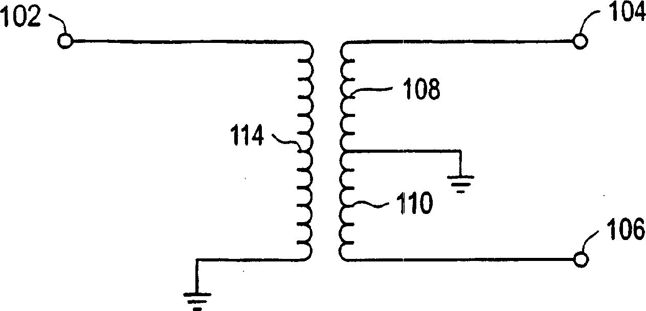
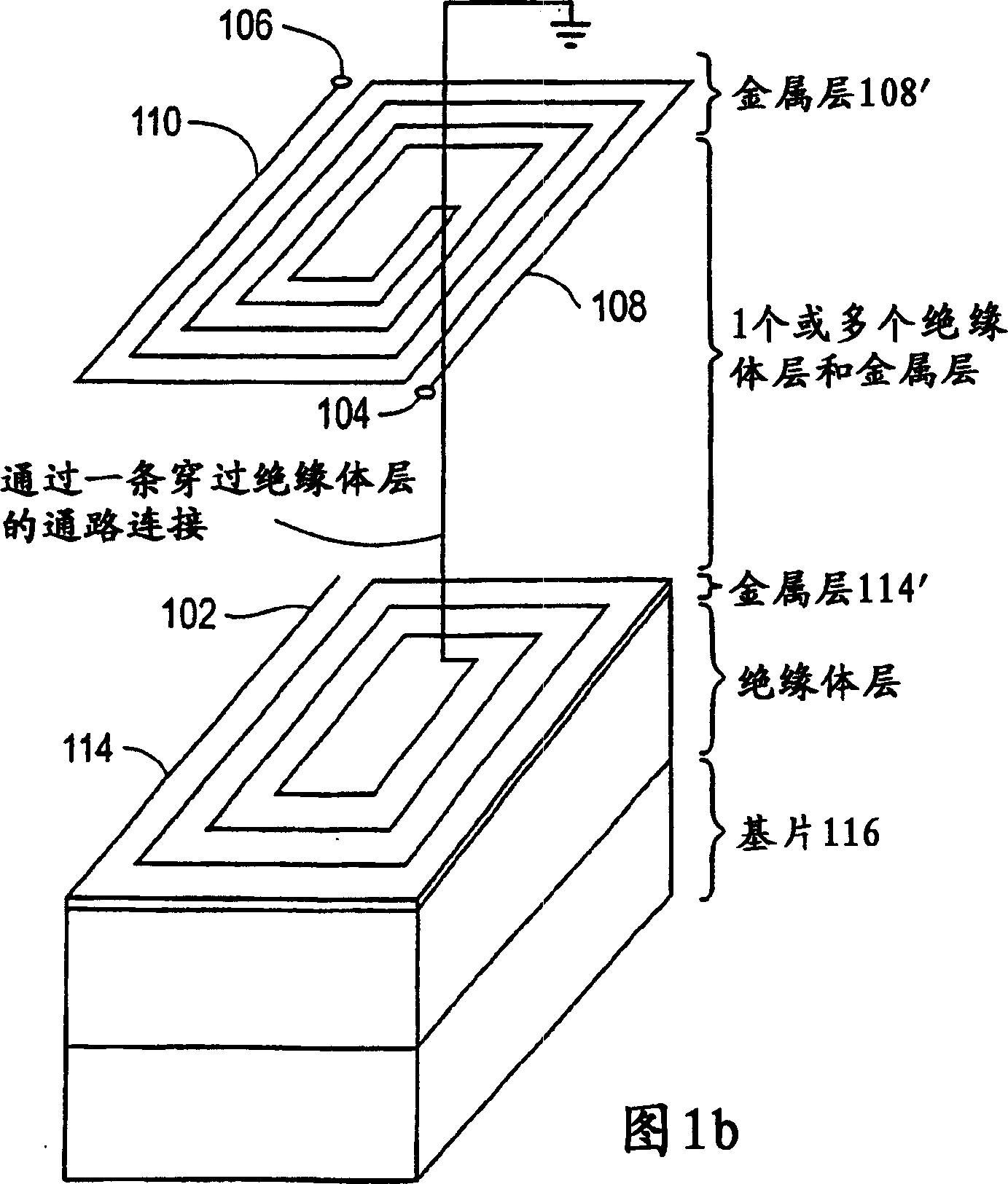
[0018] Figure 1a shows a circuit representation of a balun. Balun 100 includes inductor 114 and inductors 108 and 110 . Inductors 108 and 110 are DC decoupled but also magnetically coupled to inductor 114 to allow ...


PUM


Abstract

A method for producing an on-chip signal transforming device. The method includes providing a substrate, and laying a first conductive layer above the substrate, wherein the first conductive layer has a plurality of interleaved inductors. The method then includes laying a second conductive layer above the substrate, wherein the second conductive layer has at least one inductor.

Description

technical field [0001] The present invention relates generally to integrated circuit devices, and more particularly to baluns and transformers fabricated on integrated circuit chips. Background technique [0002] Devices that previously resided on printed circuit boards (PCBs) are increasingly being integrated on integrated circuit (IC) chips for reliability, performance, and cost reasons. Transformers, inductors, and baluns are examples of devices that migrate to IC chips. [0003] Due to the relatively noisy environment on an IC chip, many of the signals on the chip are typically differential or double-ended. Differential signals provide good common-mode rejection of noise; noise typically affects both halves of a differential signal in the same way, and since information is contained in the difference of the two signal halves, despite the addition of Even noise does not change significantly. [0004] A balun is an example of a device that takes a single-ended signal an...

Claims


Application Information

Patent Timeline
IPC IPC(8): H01F41/04H01F19/06H01L21/822H01L27/04H03H7/42
CPCH03F3/45183H03F2200/541Y10T29/4902Y10T29/49155H03H7/42H03F2203/45662
Inventor 奇克·P.·俞
Owner ATHEROS COMM INC
Learn More