Supercharge Your Innovation With Domain-Expert AI Agents!

Semiconductor manufacturing process

A manufacturing method and semiconductor technology, applied in semiconductor/solid-state device manufacturing, semiconductor devices, electric solid-state devices, etc., can solve the problems of lower packaging efficiency, large volume, lower pass rate of optical sensing modules, etc., to save time and cost , to avoid the effect of particle pollution

Inactive Publication Date: 2005-04-20
UNITED MICROELECTRONICS CORP
View PDF0 Cites 2 Cited by
  • Summary
  • Abstract
  • Description
  • Claims
  • Application Information

AI Technical Summary

Problems solved by technology

[0005] It is worth noting that after the packaging of the existing light sensing element is completed, a lens 130 must be assembled on the light sensing module to increase the luminous flux, and an infrared blocking layer (IR Cutting Film) 140 must be arranged between the lens and the light. Between the sensing modules, it is used to block the irradiation of non-visible light, and the lens 130 and the infrared blocking layer 140 must be fixed with a holde

Method used


Image

  • Semiconductor manufacturing process
  • Semiconductor manufacturing process
  • Semiconductor manufacturing process

Examples


Embodiment Construction

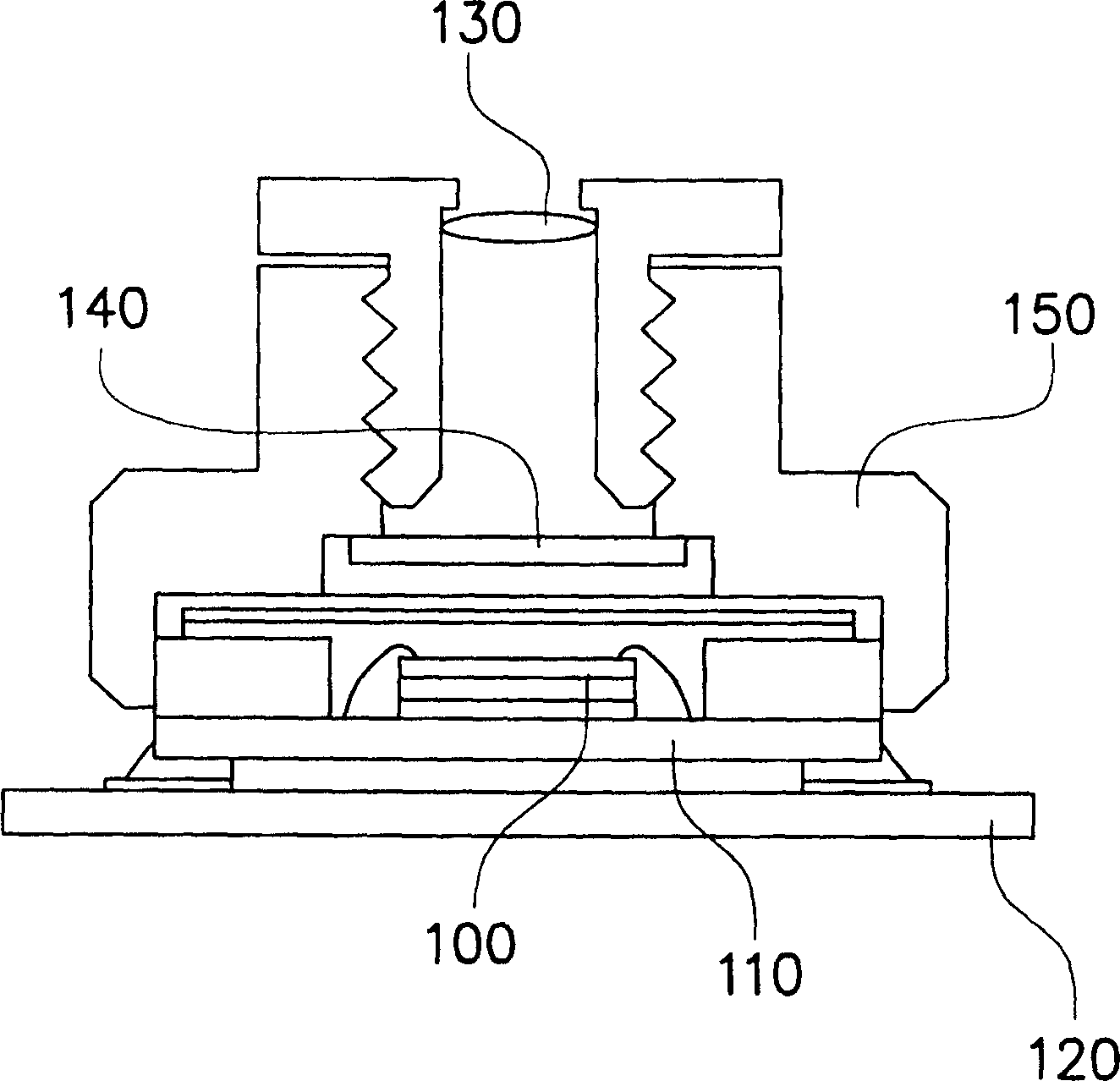
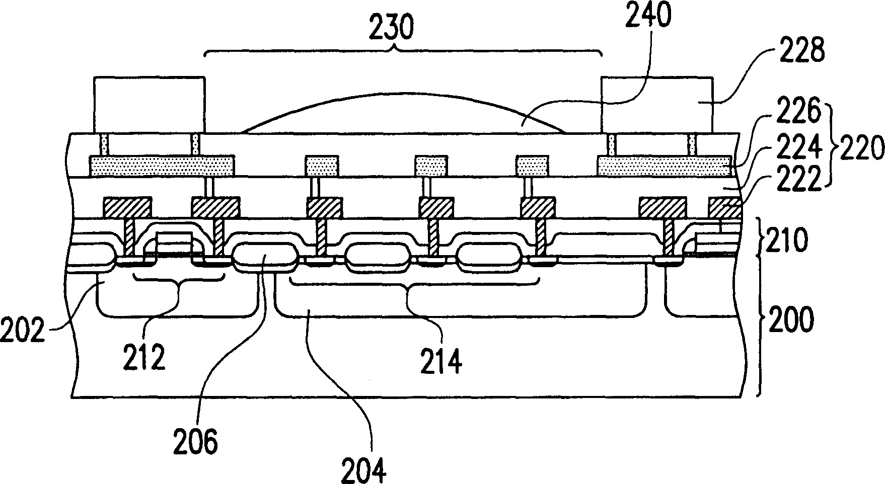
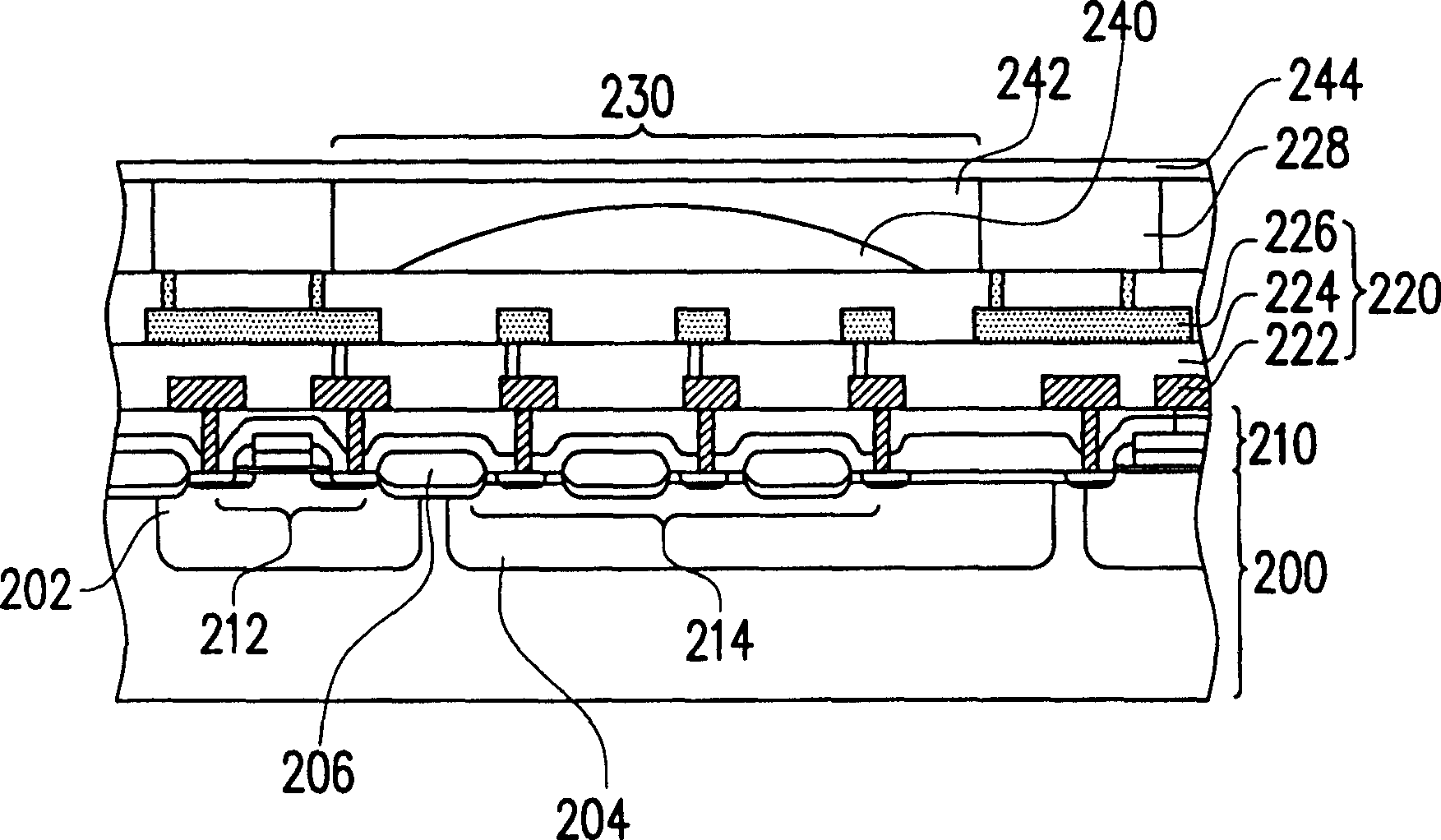
[0029] Please refer to Figure 2A ~2E, which sequentially show a schematic flow chart of a semiconductor manufacturing method according to a preferred embodiment of the present invention. Please refer to Figure 2A , a wafer 200 is provided, and the active element 212 and the photodiode array 214 of the active layer 210 are formed on the wafer 200 through a multi-channel mask process, wherein the active element 212 is, for example, a metal oxide semiconductor (MOS) transistor, which is commonly used There are PMOS transistors or CMOS transistors. The PMOS transistor is generally located on the surface of the silicon substrate (ie wafer) 200 of the N-type well 202, and the photodiode array 214 may be located on the surface of the silicon substrate 200 of the P-type well 204, and then a gate oxide layer ( gate oxide) 206 to separate the active device 212 from the photodiode array 214 . Then use the second masking process to determine the contact window of the gate (source and...


PUM


Abstract

This invention discloses a semiconductor manufacturing method combining a shut-off layer technology on the first section of a semiconductor, among which, the shut-off layer can be formed on the curved face of the micro-lens first then to cover a shut-off layer on the surface of the protection layer, and finally, the volume of a formed photo-sensing module reaches to the minimum and the continuous packaging technology can save time and cost.

Description

technical field [0001] The present invention relates to a semiconductor element, and in particular to a structure of a light sensing element and a manufacturing method thereof. Background technique [0002] The semiconductor industry is one of the fastest-growing high-tech industries in recent years. With the rapid development of electronic technology and the emergence of high-tech electronic industries one after another, more humanized and functional electronic products are constantly being introduced. [0003] As far as the front-end process of semiconductor components is concerned, at least five masks will be used in the entire production, which are used to define the circuit pattern of the active region, gate structure, metal layer and source / drain contact window, and metal interconnection. And the welding pad (bonding pad) window. In addition, for the fabrication of photosensitive devices, after the ion implantation of the source and drain electrodes, an additional mas...

Claims


Application Information

Patent Timeline
IPC IPC(8): H01L21/82H01L27/14H01L31/00
Inventor 孙正光李光兴潘瑞祥
Owner UNITED MICROELECTRONICS CORP
Features
  • R&D
  • Intellectual Property
  • Life Sciences
  • Materials
  • Tech Scout
  • Unparalleled Data Quality
  • Higher Quality Content
  • 60% Fewer Hallucinations
Learn More