Supercharge Your Innovation With Domain-Expert AI Agents!

Sealing structure of light emitting diodes

A technology of light-emitting diodes and packaging structures, applied in the direction of electrical components, circuits, semiconductor devices, etc., to achieve the effects of smaller materials, shorter conductive paths, and smaller base areas

Inactive Publication Date: 2005-10-12
EVERLIGHT ELECTRONICS
View PDF0 Cites 1 Cited by
  • Summary
  • Abstract
  • Description
  • Claims
  • Application Information

AI Technical Summary

Problems solved by technology

[0005] However, as in the above-mentioned existing packaging structure, the conductive film needs to surround the top surface, side surface and bottom surface of the base, so there are many restrictions on the size design of the structure miniaturization

Method used


Image

  • Sealing structure of light emitting diodes
  • Sealing structure of light emitting diodes
  • Sealing structure of light emitting diodes

Examples


Embodiment Construction

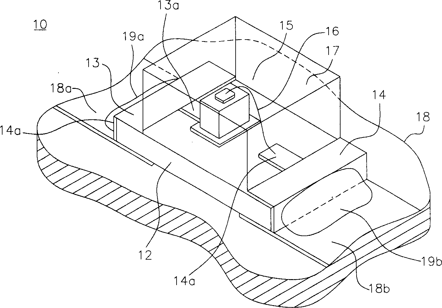
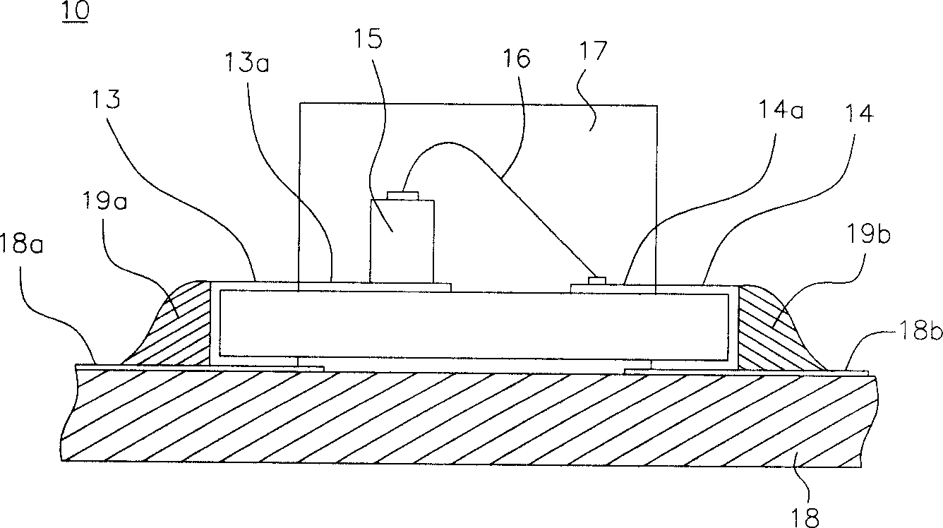
[0038] In order to further miniaturize the packaging structure of the light emitting diode, the present invention drills a through hole in the base, and forms a conductive column in the through hole to replace the conductive film in the existing packaging structure. Because the conductive thin film in the existing packaging structure needs to surround the top surface, side surface and bottom surface of the base, there are many restrictions on the size design of the structure miniaturization.

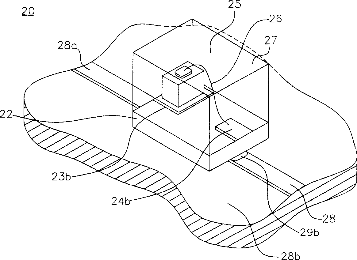
[0039] Please refer to Figure 2A and Figure 2B , which respectively show a schematic perspective view and a schematic cross-sectional view of a light emitting diode packaging structure according to a preferred embodiment of the present invention. In this embodiment, two through holes 23 , 24 are formed on the base 22 of the diode package structure 20 , and conductive posts are formed therein. In the practice of manufacturing the conductive pillars, the top ends 23 b and 24 b of the c...


PUM


Abstract

The invention consists of a base with several through-holes. With chemical plating process, the conducting pole is formed in each through-hole. The electrode of light emitting diode is separately connected with each conducting pole. The epoxy resin is used to package the light emitting diode in it to form a moulding component. The packaged light emitting diode is welded in connection on board. The invention can shorten the distance of circuit between light emitting diode and main board.

Description

technical field [0001] The invention relates to a packaging structure of a light emitting diode, in particular to a packaging structure of a light emitting diode fixed on a carrier board by means of surface adhesion technology. Background technique [0002] In recent years, the use of light-emitting diode components in the lighting field has grown exponentially. For example, LEDs are widely used in cell phones, personal digital assistants (PDAs), and other electronic products. [0003] Please refer to Figure 1A and 1B , which respectively show a three-dimensional schematic view and a schematic cross-sectional view of a conventional light emitting diode packaging structure. The carrier board 18 is a printed circuit board in electronic products, such as a motherboard in a mobile phone. The light emitting diode package structure 10 is respectively soldered to the conductive ends 18a / 18b on the carrier board 18 by means of solders 19a / 19b. One end of the LED chip 15 is conn...

Claims


Application Information

Patent Timeline
Patent Type & Authority Applications(China)
IPC IPC(8): H01L33/48H01L33/62
Inventor 林裕胜
Owner EVERLIGHT ELECTRONICS
Features
  • R&D
  • Intellectual Property
  • Life Sciences
  • Materials
  • Tech Scout
  • Unparalleled Data Quality
  • Higher Quality Content
  • 60% Fewer Hallucinations
Learn More