A resistive variable memory and its preparation method

A resistive variable memory and resistive variable technology, applied in the field of memory, can solve problems such as misreading and miswriting of stored information, and reducing the reliability of stored data.

Active Publication Date: 2020-06-09
JIMEI UNIV
View PDF5 Cites 0 Cited by
  • Summary
  • Abstract
  • Description
  • Claims
  • Application Information

AI Technical Summary

Problems solved by technology

There are many evaluation criteria for the storage performance of resistive variable memory, the most important of which are the switch resistance ratio and stability. If the switch resistance ratio and stability of the memory are poor, it may lead to misreading and miswriting of stored information, reducing the Reliability of stored data

Method used


Image

  • A resistive variable memory and its preparation method
  • A resistive variable memory and its preparation method
  • A resistive variable memory and its preparation method

Examples


preparation example Construction

[0023] The present invention provides a method for preparing a resistive random access memory, which includes the following steps:

[0024] Deposit resistive material on the bottom electrode to form an amorphous resistive layer;

[0025] Preparing a nanotube array on the amorphous resistive layer to form a shielding layer;

[0026] Performing oxygen plasma enhanced annealing treatment on the overall structure forming the shielding layer to convert the amorphous resistive layer into a highly crystalline array region;

[0027] The shielding layer is removed, and a top electrode is prepared on the surface of the high crystal array area to obtain a resistive random access memory.

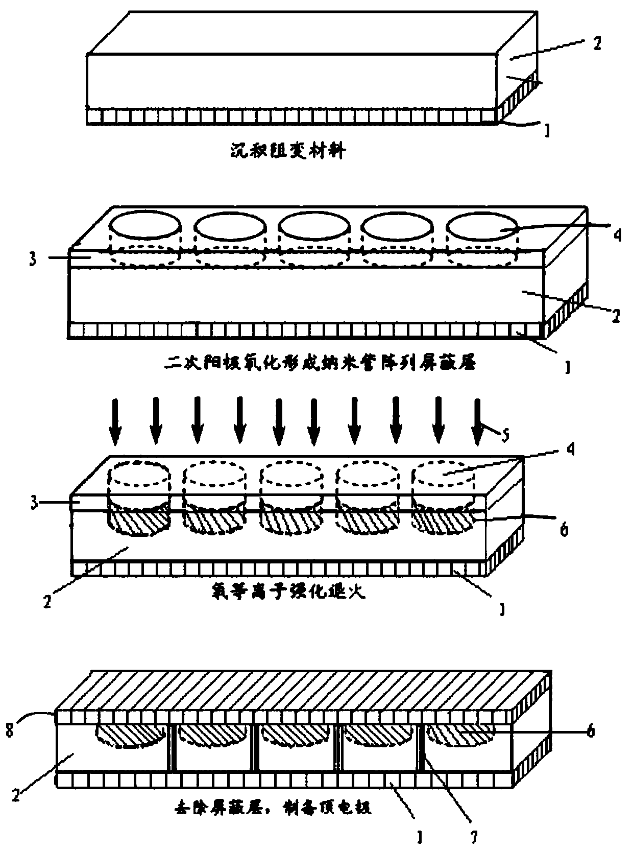
[0028] In order to clearly illustrate the scheme of the present invention, the following specific embodiments refer to figure 1 The process diagram shown is explained:

[0029] In the present invention, a resistive material is deposited on the bottom electrode 1 to form an amorphous resistive layer 2. In the pres...

Embodiment 1

[0047] according to figure 1 The schematic diagram of the process flow shown to prepare the resistive random access memory, the specific steps are as follows:

[0048] On the surface of the silicon substrate, a Cr / Cu / Cr metal film is prepared by the DC sputtering method as the bottom electrode of the resistive random access memory; during deposition, the deposition process parameters are controlled as follows: a chromium target is used as the sputtering target, and the substrate temperature does not exceed 100°C (Controlled at 90°C, the substrate temperature in the following steps is the same), sputtering power 100W, sputtering time 3min and using copper target as sputtering target, substrate temperature below 100°C, sputtering power 100W, sputtering time 2min; After deposition, a Cr / Cu / Cr bottom electrode is obtained, wherein the thickness of a single layer of Cr is 10 nm, and the thickness of Cu is 10 nm;

[0049] Continue to use radio frequency magnetron sputtering to prepare a ...

Embodiment 2~3

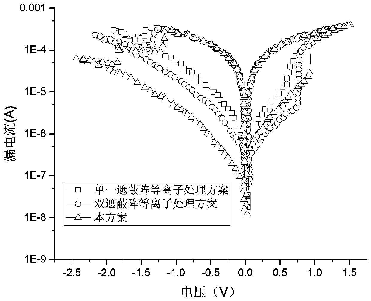
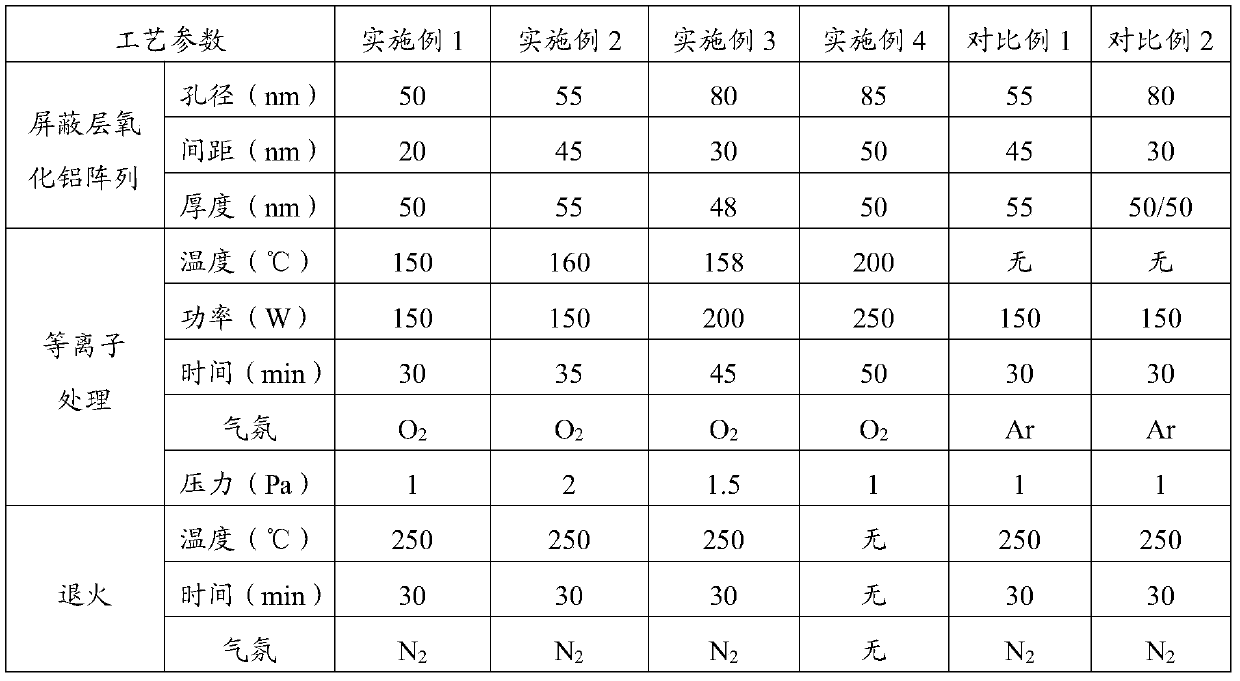
[0059] The resistive random access memory was prepared in the manner of Example 1, except that the thickness of each material layer deposited and the annealing process parameters are different, which are specifically listed in Table 1.


PUM

PropertyMeasurementUnit
thicknessaaaaaaaaaa
diameteraaaaaaaaaa
depthaaaaaaaaaa

Abstract

The invention belongs to the technical field of memory, and in particular relates to a resistive variable memory and a preparation method thereof. The preparation method provided by the present invention includes the following steps: depositing a resistive switchable material on the bottom electrode to form an amorphous resistive switchable layer; preparing a nanotube array on the amorphous resistive switchable layer to form a shielding layer; The overall structure of the shielding layer is subjected to oxygen plasma enhanced annealing treatment to convert the amorphous resistive layer into a highly crystalline array region; the shielding layer is removed, and a top electrode is prepared on the surface of the highly crystalline array region to obtain Resistive memory. The results of the examples show that the stability of the resistive memory provided by the present invention is significantly improved. After 500 resistive cycles, the maximum change in the size of the storage window is about -1.7%. After 3000 cycles, the maximum change in the size of the storage window is It is about ‑6.3%, showing good stability.

Description

Technical field [0001] The invention belongs to the technical field of memory, and specifically relates to a resistive random access memory and a preparation method thereof. Background technique [0002] Memory undoubtedly occupies a very important position in today's information age. With the continuous improvement of semiconductor technology, resistance random access memory (RRAM) is getting more and more attention. RRAM has the technical advantages of simple preparation process, high density, high integration, fast programming speed, reliable and stable performance, low energy consumption and low operating voltage. The most important thing is that RRAM is compatible with CMOS (Complementary Metal Oxide Semiconductor) process. Therefore, RRAM has become one of the most powerful competitors for next-generation memory. [0003] The core of the resistive random access memory is a metal / medium / metal (MIM) structure, which relies on the resistive effect of the intermediate dielectri...

Claims


Application Information

Patent Timeline
Patent Type & Authority Patents(China)
IPC IPC(8): H01L45/00
CPCH10N70/24H10N70/8833H10N70/041H10N70/011
Inventor 徐文彬李明逵
Owner JIMEI UNIV
Why Eureka
Try Eureka