Cleaning clamp for wafer carrying bench of semiconductor machine

A wafer stage, semiconductor technology, applied in semiconductor/solid-state device manufacturing, electrical components, circuits, etc., can solve the problems of difficult removal of impurities, reduced cleaning quality, and deep wafer stage depth.

Inactive Publication Date: 2006-05-10
POWERCHIP SEMICON CORP
View PDF0 Cites 7 Cited by
  • Summary
  • Abstract
  • Description
  • Claims
  • Application Information

AI Technical Summary

Problems solved by technology

[0005] 1. In the current cleaning method of the wafer carrier, because the semiconductor machine has a very low space for wiping, and the depth of the wafer carrier is deep, it is easy to have dead spots that are not easy to clean.
[0006] 2. The existing wafer stage cleaning methods often increase the complexity and difficulty of cleaning due to insufficient lighting, thereby reducing the cleaning quality and affecting the yield of subsequent wafer manufacturing processes
[0007] 3. The existing wafer carrier cleaning method, due to the manual wiping method, encounters highly viscous impurities, which are difficult to remove and affect the yield of the subsequent wafer manufacturing process.
[0008] 4. The existing wafer carrier cleaning method cannot quickly remove impurities when encountering precision components next to the wafer carrier, and it is easy to cause damage to the machine if you are not careful

Method used


Image

  • Cleaning clamp for wafer carrying bench of semiconductor machine
  • Cleaning clamp for wafer carrying bench of semiconductor machine

Examples


Embodiment Construction

[0027] In order to further recognize and understand the features, objectives and functions of the present invention, the accompanying drawings are hereby described in detail.

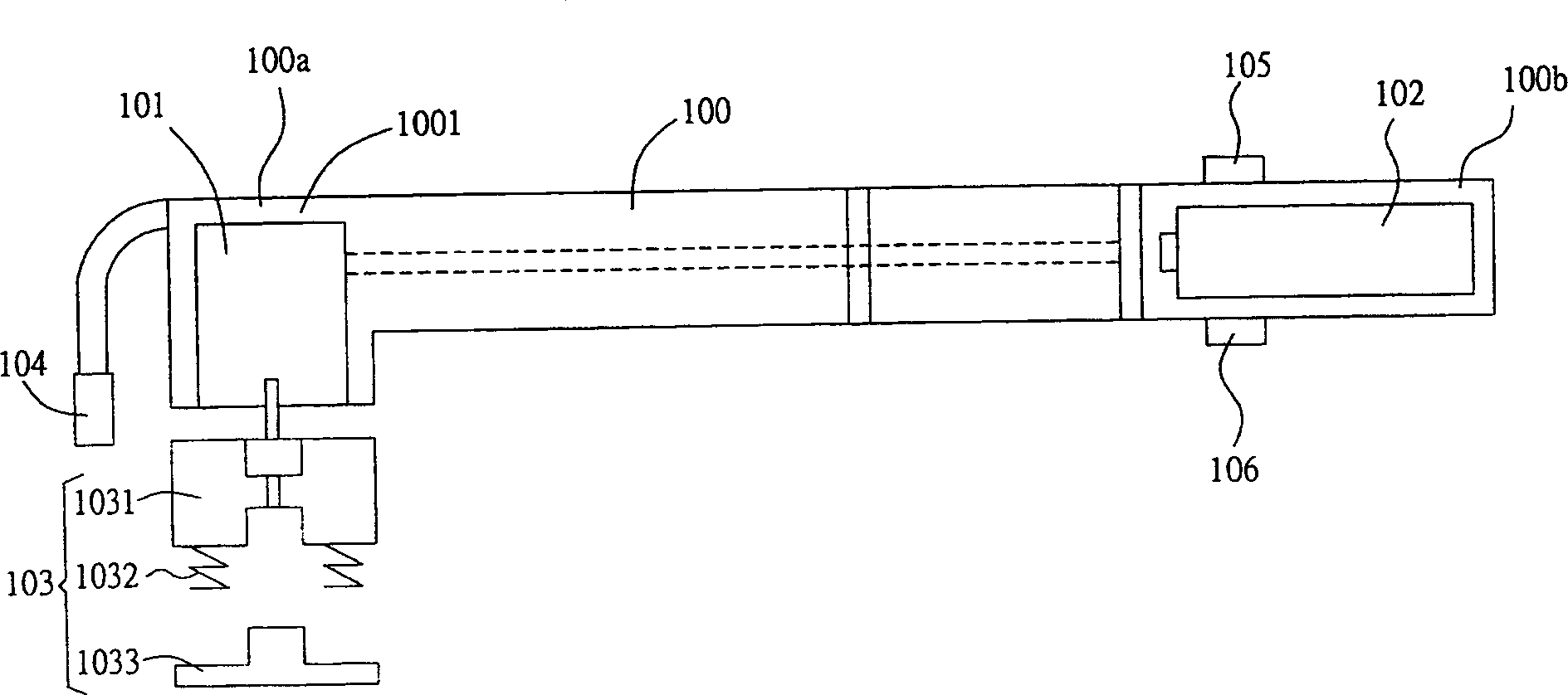
[0028] Such as figure 1 As shown, it is a schematic diagram of a preferred embodiment of the wafer stage cleaning jig of the semiconductor machine of the present invention, wherein the cleaning jig of the present invention mainly includes: a main body 100, a driving device 101 located in the main body 100, and a power supply The supply device 102 , and a cleaning module 103 interconnected with the driving device 101 and the power supply device 102 . , and the main body part 100 has a corresponding cleaning module end 100a and a handle end 100b, and the cleaning module is arranged on the cleaning module end 100a. In addition to fixing the length of the fixture between the cleaning module end 100a and the handle end 100b, for example, a telescopic rod can be used to freely adjust the length of the telesc...


PUM


Abstract

This invention relates to semiconductor crystal load bench clearing clamper, which comprises one body part, one drive device, one power supply device and one clearing module composed of one rotation base, one spring element and one clear rotation disc, wherein, the body part can be adjusted length with one capacity space located in the space to provide one power; the power supply device is coupled to the drive device to provide drive device electricity source; the rotation socket is set near to drive device through spring element connected with clearing disc by drive device to provide power to make the disc clean semiconductor mixtures.

Description

technical field [0001] The invention relates to a wafer carrier cleaning jig of a semiconductor machine, in particular to a freely retractable cleaning jig used for cleaning the wafer carrier of a semiconductor machine. Background technique [0002] When there are impurities (Particles) on the Wafer Stage of the exposure machine, it will cause the wafer to be out of focus (Defocus). At this time, the machine must stop production immediately to remove the impurities on the wafer stage. [0003] The current commonly used method is to use a dust-free cloth dipped in alcohol to wipe the wafer stage, and use the manual method of lighting with a flashlight. However, due to the 12-inch semiconductor machine currently used, there are many precision components near the wafer stage, and The space available for wiping is very low, coupled with the deep depth of the wafer stage, it often causes trouble when the wiper wipes the wafer stage, and even if the wiper is very careful, there is...

Claims


Application Information

Patent Timeline
Patent Type & Authority Applications(China)
IPC IPC(8): H01L21/00
Inventor 王宏祺郭宗铭林炜烽
Owner POWERCHIP SEMICON CORP
Why Eureka
Try Eureka