Check patentability & draft patents in minutes with Patsnap Eureka AI!

Thin film transistor array panel

A thin film transistor and array board technology, applied in the field of thin film transistor array boards, can solve problems such as TFT characteristic degradation

Inactive Publication Date: 2006-08-30
SAMSUNG ELECTRONICS CO LTD
View PDF0 Cites 8 Cited by
  • Summary
  • Abstract
  • Description
  • Claims
  • Application Information

AI Technical Summary

Problems solved by technology

These protrusions can prevent the flow of electric current, and this effect can lead to degradation of TFT characteristics, resulting in visible defects (such as horizontal and vertical stripes) in the display

Method used


Image

  • Thin film transistor array panel
  • Thin film transistor array panel
  • Thin film transistor array panel

Examples


Embodiment Construction

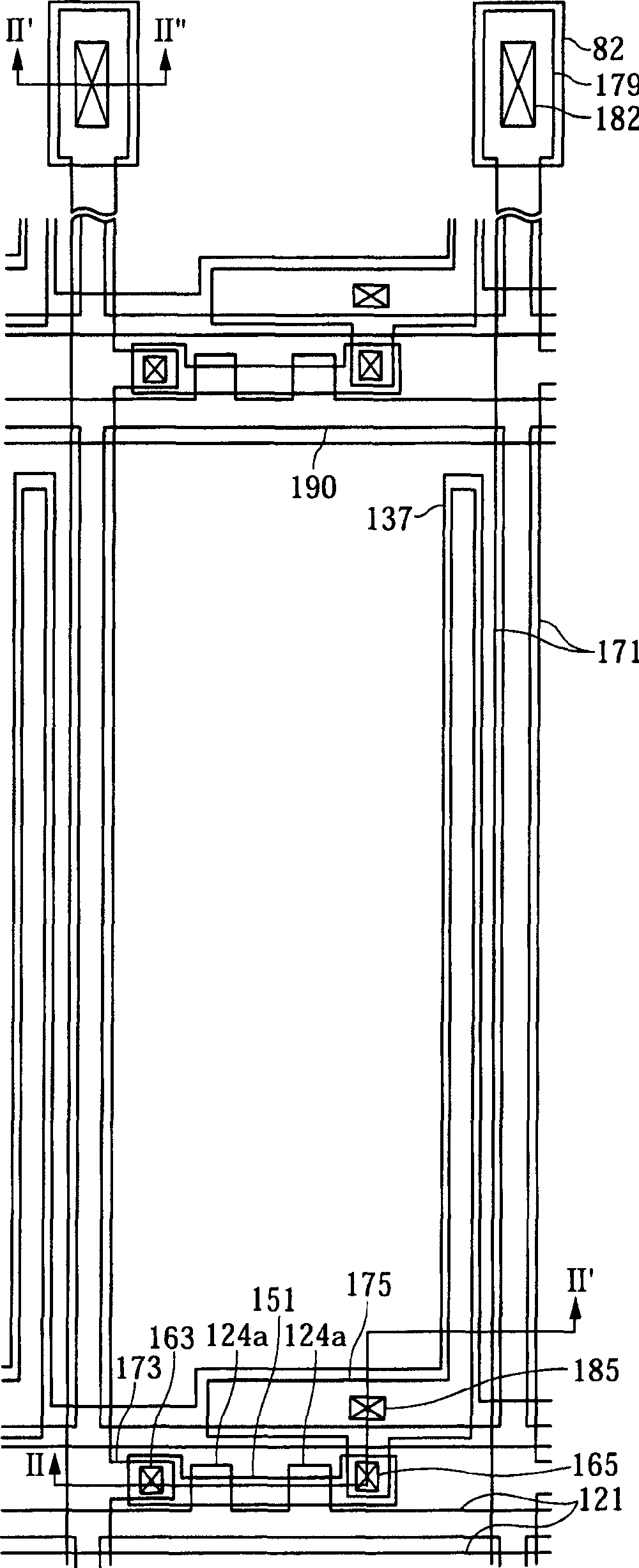
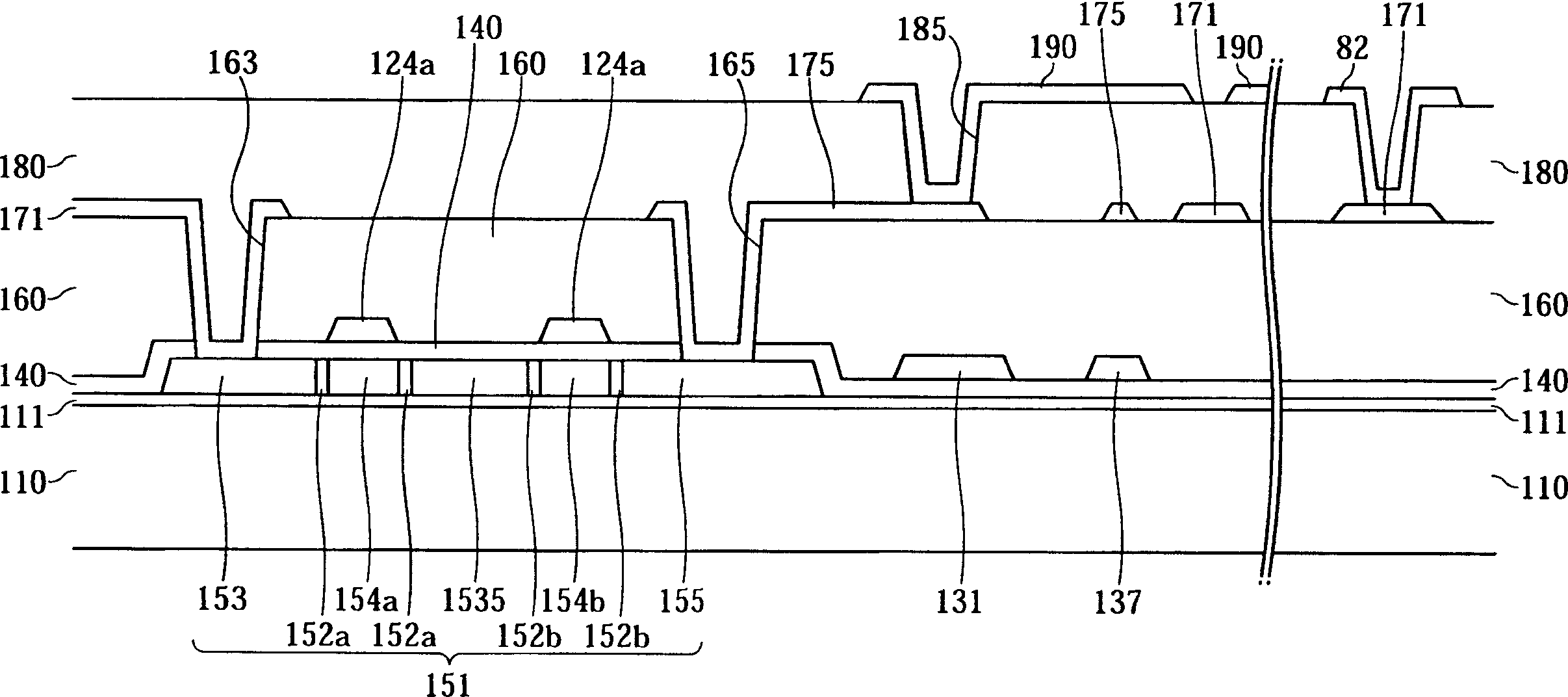
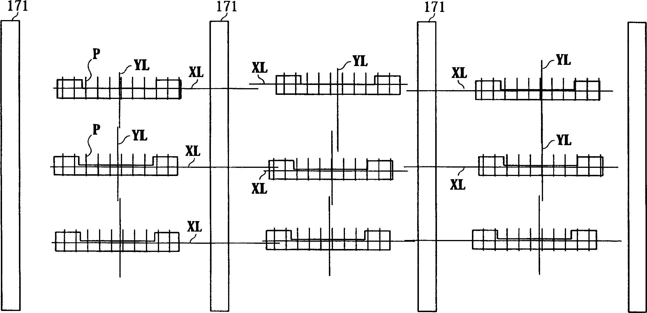
[0041] figure 1 It is a layout diagram of a TFT array panel for LCD according to an embodiment of the present invention; figure 2 yes figure 1 The cross-sectional view of the TFT array plate taken along section lines II-II' and II'-II"; image 3 is a layout diagram showing the centerlines of the horizontal and vertical axes of semiconductor islands disposed on a figure 1 with 2 Among multiple pixels in the TFT array panel shown; Figure 4 is a layout diagram showing relative positions between protrusions and lightly doped drain regions formed in semiconductor islands provided in a semiconductor island according to an embodiment of the present invention. figure 1 with 2 Among multiple pixels in the TFT array board; Figure 5 is a layout diagram showing relative positions among protrusions, gate electrodes, and channel regions formed in semiconductor islands provided in a plurality of pixels in a TFT array panel according to another embodiment of the present invention ; ...


PUM


Abstract

A thin film transistor (TFT) array display panel is provided, which includes: a substrate; a plurality of semiconductor islands formed on the substrate; a gate insulating layer covering the semiconductor islands; a plurality of gate lines formed on the gate insulating layer; a plurality of data lines connected to the source regions and formed on the gate insulating layer; and a plurality of pixel electrodes connected to the drain regions. the number or at grain boundaries of the portion of the semiconductor that is selected as the gate region is varied (different, unequal) among the semiconductors in the same column of the array which prevents visible stripes due to current leakage caused by protrusions. The position of each semiconductor island is varied among semiconductors in the same column of the array. Alternatively, the position of the gate electrode which defines the gate region of the semiconductor island is varied among uniformly positioned semiconductors in the same column of the array.

Description

technical field [0001] The invention relates to a thin film transistor array panel using polysilicon as a semiconductor. Background technique [0002] In a flat panel display including a plurality of pixels such as a liquid crystal display (LCD) or an organic light emitting diode display (OLED), a thin film transistor (TFT) array panel is used as a substrate of a data driving circuit configured to drive each pixel independently. [0003] A liquid crystal display (LCD) includes two panels (substrates) each provided with field generating electrodes such as a pixel electrode and a common electrode, with a liquid crystal (LC) layer interposed therebetween. The LCD displays images by applying a voltage to the field generating electrodes to generate an electric field across the LC layer, which controls the orientation of LC molecules in the LC layer to adjust polarization of incident light. [0004] An organic light emitting diode display (OLED) is a self-emissive display device ...

Claims


Application Information

Patent Timeline
IPC IPC(8): H01L27/12
CPCA47G1/141B32B25/10B32B29/02G02C13/006
Inventor 姜珍奎
Owner SAMSUNG ELECTRONICS CO LTD
Features
  • R&D
  • Intellectual Property
  • Life Sciences
  • Materials
  • Tech Scout
  • Unparalleled Data Quality
  • Higher Quality Content
  • 60% Fewer Hallucinations
Learn More