

Formation of silicon nitride film by using atomic layer deposition method
一种氮化硅膜、硅氮化物的技术,应用在涂层、气态化学镀覆、金属材料涂层工艺等方向,能够解决不能实现应力强度、氮化硅膜湿蚀刻速率大、氮化硅膜膜应力低等问题
- Summary
- Abstract
- Description
- Claims
- Application Information
AI Technical Summary
Problems solved by technology
Method used
Image

Examples
Embodiment Construction
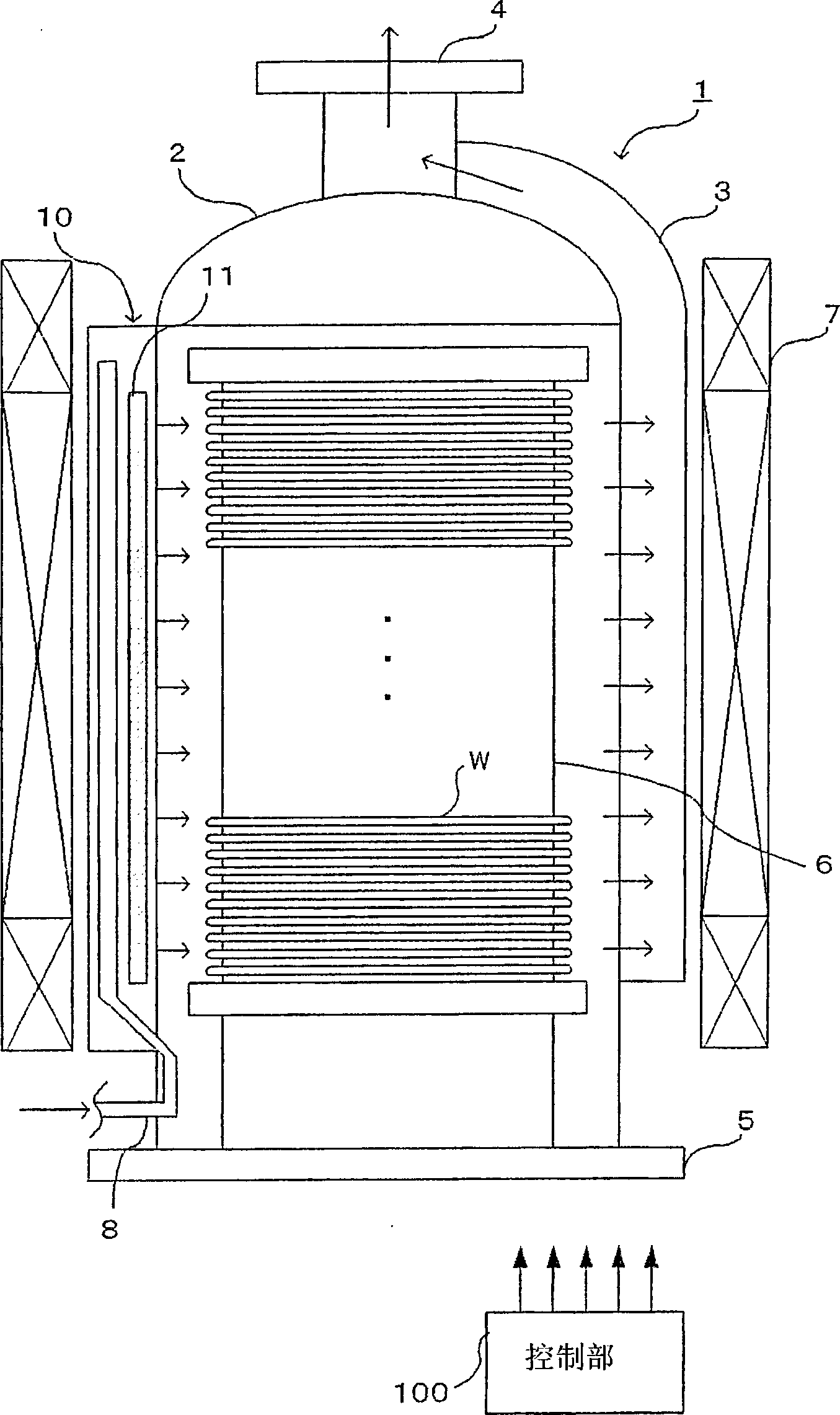
[0023] Preferred embodiments of the present invention will be described below with reference to the drawings. In the exemplary embodiments described below, a batch type vertical processing apparatus is used as the silicon nitride film forming apparatus.
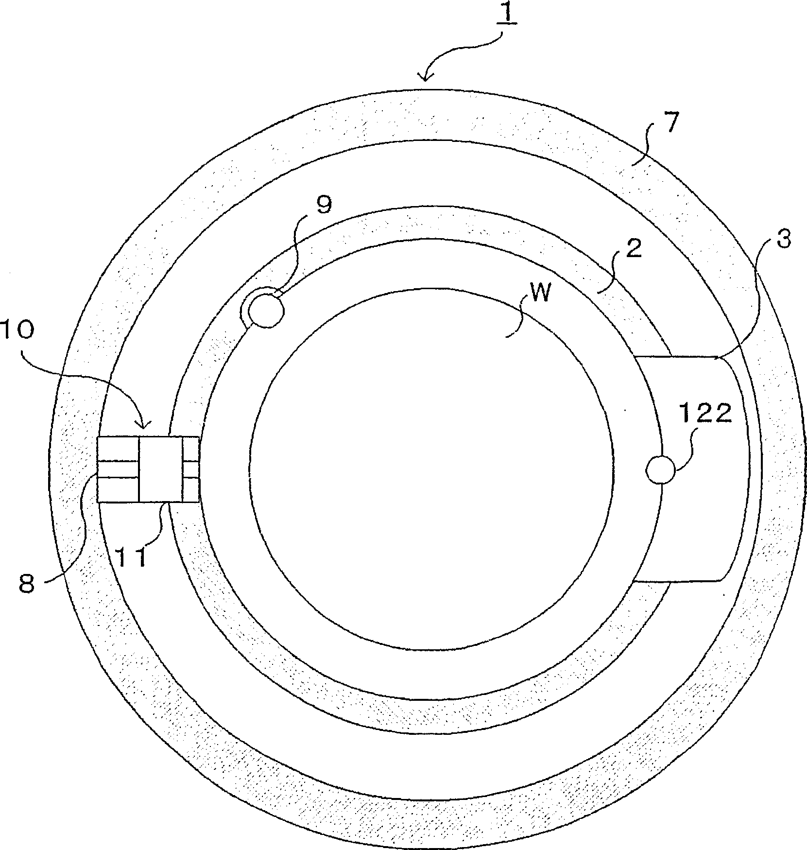
[0024] Such as figure 1 As shown, the longitudinal direction of the processing device 1 has a substantially cylindrical reaction tube 2 facing the vertical direction. The reaction tube 2 is made of a material excellent in heat resistance and corrosion resistance, for example, quartz.
[0025] The exhaust unit 3 is disposed on one side of the reaction tube 2 and is used to exhaust the gas in the reaction tube 2 . The exhaust part 3 is provided on the side wall of the reaction tube 2 and communicates with the reaction tube 2 through an opening (not shown) extending upward along the reaction tube 2 . The upper end of the exhaust part 3 is connected to the exhaust port 4 arranged at the upper part of the reaction tube 2 . An ...
PUM
| Property | Measurement | Unit |
|---|---|---|
| pressure | aaaaa | aaaaa |
| pressure | aaaaa | aaaaa |
Abstract
Description
Claims
Application Information