A flowable chemical vapor deposition method for silicon nitride thin films

A silicon nitride film, flow chemistry technology, applied in the manufacture of electrical components, circuits, semiconductor/solid-state devices, etc., can solve the problems of high proportion, reduce H-Si bond density, etc., achieve good uniformity and reduce wet etching rate , the effect of high coverage

Active Publication Date: 2020-12-22
合肥安德科铭半导体科技有限公司
View PDF7 Cites 0 Cited by
  • Summary
  • Abstract
  • Description
  • Claims
  • Application Information

AI Technical Summary

Problems solved by technology

In the WO2016065219A1 patent application, the precursors bis(disilylamino)silane (IIB) and tri(ethylsilyl)amine that can reduce the H-Si bond density are disclosed. Such TSA dimers or trimers Although the hydrogen content can be reduced, the ratio of H:Si is still very high, reaching 14:5, which still cannot meet the demand.

Method used


Image

  • A flowable chemical vapor deposition method for silicon nitride thin films
  • A flowable chemical vapor deposition method for silicon nitride thin films
  • A flowable chemical vapor deposition method for silicon nitride thin films

Examples


Embodiment 1

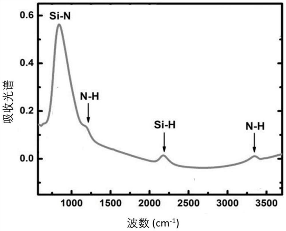
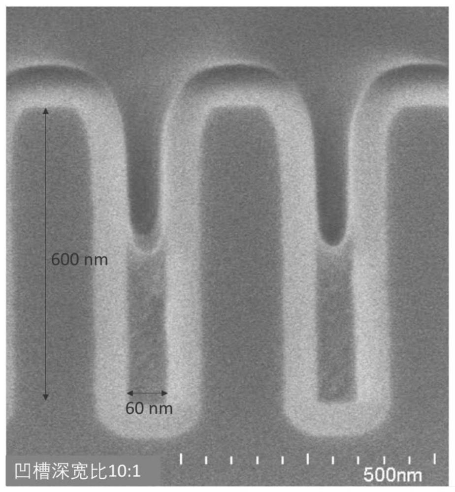
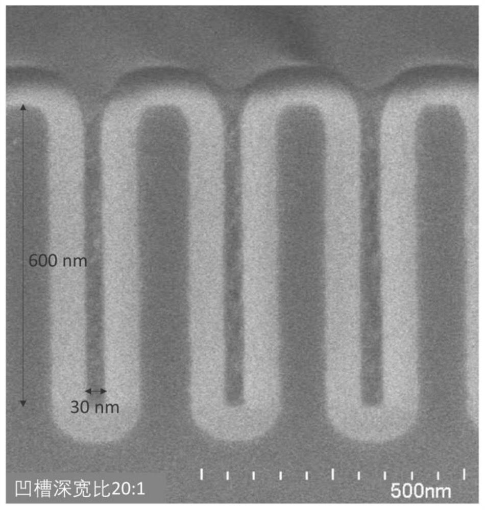
[0062] At a temperature of 20°C, the cyclosilane is reacted with a nitrogen-containing compound, and is deposited to a medium resistivity (that is, a resistivity of 8-12Ω·cm, such as 8Ω·cm, 10Ω·cm, cm, 12Ω cm) single crystal silicon wafer substrates and silicon pattern wafers, a flowable silicon nitride film is formed until the grooves of the substrate are filled, and then annealed at 700°C for 3 hours to finally obtain a dense Silicon nitride film.

[0063] The cyclosilane is cyclopentasilane, cyclohexasilane, cyclooctylsilane or trimethylsilylcyclotrisilazane. The nitrogen-containing compound is ammonia, nitrogen / hydrogen mixed gas, hydrazine or nitrogen trifluoride. A pre-deposition treatment is performed on the above-mentioned single crystal silicon wafer substrate in advance, and the specific pre-deposition treatment may be plasma treatment, heat treatment, chemical treatment, ultraviolet light exposure, and electron beam bombardment.

[0064] The film deposition descri...

Embodiment 2

[0066] The difference from Example 1 is that the flowable silicon nitride film is annealed at 900° C. for 1 h, and finally a dense silicon nitride film is obtained. The process parameters of the plasma flowable chemical vapor deposition are as follows: the flow rate of cyclosilane is 5000 mg / min, the flow rate of nitrogen-containing compound is 1000 sccm, and the in-situ plasma power density is 3.5 W / cm 2 , the pressure is 12Torr.

Embodiment 3

[0068] The difference from Example 1 is that the flowable silicon nitride film is treated with ultraviolet light for 12 minutes, and then cured by bombardment with nitrogen-containing ion beams at 400°C. Repeat the above steps until a dense silicon nitride film with a certain thickness is obtained. The process parameters of the plasma flowable chemical vapor deposition are as follows: the flow rate of cyclosilane is 2000 mg / min, the flow rate of nitrogen-containing compound is 600 sccm, and the in-situ plasma power density is 0.3W / cm 2 , the pressure is 5Torr.

[0069] The resulting dense silicon nitride film was immersed in a 10:1 hydrofluoric acid solution for wet etching rate measurement, and the wet etching rate was less than 10 times that of the silicon nitride film prepared by LPCVD.


PUM

PropertyMeasurementUnit
densityaaaaaaaaaa
widthaaaaaaaaaa
thicknessaaaaaaaaaa

Abstract

The invention provides a movable chemical vapor deposition method of a silicon nitride thin film with relatively low etching rate. Cyclosilane with an annular molecule structure is used as a precursor, the cyclosilane and a nitrogen-containing compound are deposited on a substrate by a deposition-curing periodic circulation mode to form the movable silicon nitride thin film until a groove of the substrate is filled. The Si-H bond density of the silicon nitride thin film is remarkably reduced, the etching speed is also greatly reduced, and seamless gap filling in a silicon wafer with a patterncan be achieved from bottom to top, the high-quality silicon nitride thin film can be formed on a blank silicon wafer, the method is more suitable for filling of a new-generation semiconductor component with high depth-to-width ratio gap, and the silicon nitride thin film is good in uniformity, good in compactness and high in convergence rate.

Description

technical field [0001] The invention relates to the technical field of silicon nitride thin films, in particular to a flowable chemical vapor deposition method for silicon nitride thin films. Background technique [0002] In semiconductor processing, since the size of the device is required to be smaller and smaller, the semiconductor usually has a high aspect ratio (HAR) structure, and gaps between the high aspect ratio structures must be filled with insulating materials. Examples of insulating materials used in gap-fill applications include shallow trench isolation, inter-metal dielectric layers, passivation layers, patterning applications, and more. Due to shrinking device geometries and lower thermal loads, seamless gapfilling of high aspect ratio structures by conventional thermal deposition processes has become increasingly difficult. [0003] Flowable chemical vapor deposition (FCVD) is a new preparation method for thin film materials, usually using aminosilane compo...

Claims


Application Information

Patent Timeline
Patent Type & Authority Patents(China)
IPC IPC(8): H01L21/02H01L21/762
CPCH01L21/02164H01L21/0217H01L21/02211H01L21/02271H01L21/02318H01L21/02337H01L21/02348H01L21/76224
Inventor 不公告发明人
Owner 合肥安德科铭半导体科技有限公司
Why Eureka
Try Eureka