Thin-film field-effect transistor with organic semiconductor requiring low operating voltages

a field-effect transistor and organic semiconductor technology, applied in transistors, thermoelectric devices, solid-state devices, etc., can solve the problems of insulator undesirable characteristics, inferior dielectric strength, mobile charges, sensitivity to humidity, etc., to facilitate charge accumulation, facilitate the filling of trap states, and move more easily

Inactive Publication Date: 2002-02-05
GLOBALFOUNDRIES INC
View PDF3 Cites 114 Cited by
  • Summary
  • Abstract
  • Description
  • Claims
  • Application Information

AI Technical Summary

Benefits of technology

It is an object of this invention is to demonstrate TFT structures that overcome the need to use high operating voltages in order to achieve the desirable combination of high field effect mobility, low threshold voltage, low sub-threshold slope, and high current modulation, without having to reduce the thickness of the insulator. Such structures contain an inorganic high dielectric constant gate insulator layer (for example, barium strontium titanate) in combination with an organic semiconductor (for example, pentacene).
optionally annealing the films at a suitable temperature in the range of 150 to 400.degree. C. to improve the film quality and enhance the dielectric constant;
Alternatively it is possible, although not expected, that the gate voltage dependence is a manifestation of the changes in the accumulated carrier concentration at the semiconductor / insulator interface. It is probable, that in organic semiconductors the extra accumulation of charge carriers facilitates the filling of trap states thereby allowing the additional carriers to move more easily without being hampered by the trapping process. We propose to facilitate charge accumulation by replacing SiO.sub.2 with an insulator that has a similar thickness but a much higher dielectric constant. In this case, a similar accumulated carrier concentration is attained as in the SiO.sub.2 case, but at much lower gate fields and thus gate voltages, with all the other parameters kept the same.

Problems solved by technology

However, that insulator exhibits some undesirable characteristics such as inferior dielectric strength, mobile charges, (G. Horowitz, F. Deloffre, F. Garnier, R. Hajlaoui, M. Hmyene, A. Yassar, Synthetic Metals, Volume 54, pg 435, 1993) and sensitivity to humidity.
Hence it is not suitable for use as a gate insulator in the fabrication of practical TFT devices.
Major drawbacks of these pentacene-based organic TFT's are high threshold voltage, high operating voltages required to achieve high mobility and simultaneously produce high current modulation (typically about 100 V when 0.4 .mu.m thick SiO.sub.2 insulator is used), and high sub-threshold slope, S, which is approximately 14 V per decade of current modulation (Y. Y. Lin, D. J. Gundlach, T. N. Jackson, 54.sup.th Annual Device Research Conference Digest, 1996, pg.
Reducing the thickness of the gate insulator would improve the above mentioned characteristics but there is a limit to the decrease of the insulator thickness, which is imposed by ease of manufacturing and reliability issues.

Method used


Image

  • Thin-film field-effect transistor with organic semiconductor requiring low operating voltages
  • Thin-film field-effect transistor with organic semiconductor requiring low operating voltages
  • Thin-film field-effect transistor with organic semiconductor requiring low operating voltages

Examples


Embodiment Construction

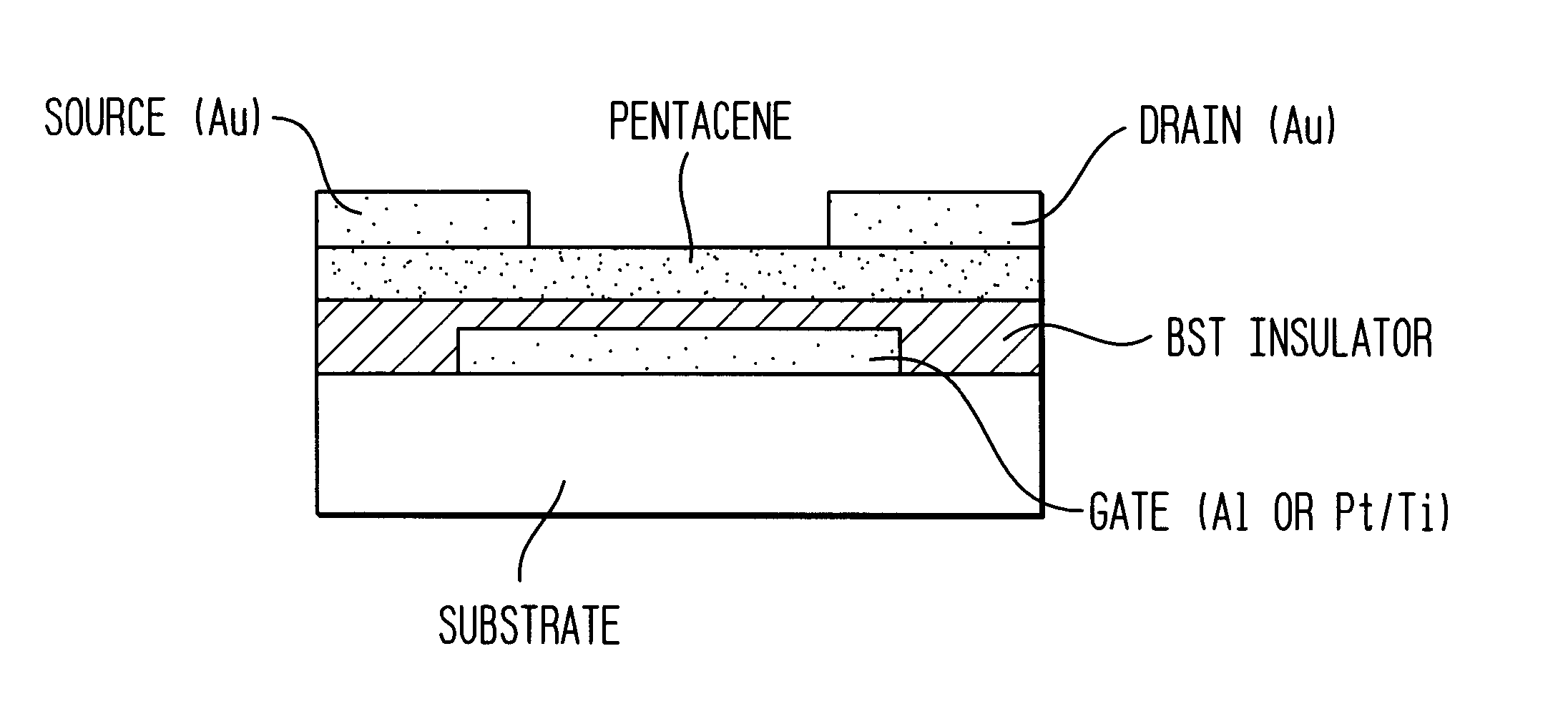
We have fabricated TFT's having as gate insulator a thin film of barium strontium titanate (BST), which was deposited using sol gel techniques. The organic semiconductor used in these devices was pentacene deposited by vacuum sublimation. The gate electrode was aluminum or a Pt / Ti bilayer while the source and drain electrodes consisted of Au. The substrates used were either quartz disks or Si wafers covered with a thermally grown SiO.sub.2 layer.

Oxidized silicon or quartz substrates were cleaned in an isopropanol bath using ultrasonic agitation and dried with nitrogen. They were then assembled with a metal mask with openings corresponding to the gate lines and placed and pumped down to high vacuum in an electron beam evaporator. Gate metallization of either 40 nm of aluminum or a bilayer of 15 nm titanium followed by 30 nm of Pt was deposited on the substrates by electron beam evaporation. The samples were unloaded from the assembly and coated with a layer of high dielectric constan...


PUM


Abstract

A thin film transistor (TFT) device structure based on an organic semiconductor material, that exhibits a high field effect mobility, high current modulation and a low sub-threshold slope at lower operating voltages than the current state of the art organic TFT devices. The structure comprises a suitable substrate disposed with he following sequence of features: a set of conducting gate electrodes covered with a high dielectric constant insulator, a layer of the organic semiconductor, sets of electrically conducting source and drain electrodes corresponding to each of the gate lines, and an optional passivation layer that can overcoat and protect the device structure. Use of high dielectric constant gate insulators exploits the unexpected gate voltage dependence of the organic semiconductor to achieve high field effect mobility levels at very low operating voltages. Judicious combinations of the choice of this insulator material and the means to integrate it into the TFT structure are taught that would enable easy fabrication on glass or plastic substrates and the use of such devices in flat panel display applications.

Description

This invention pertains to the field of organic thin film field effect transistors (TFT), in particular to flat panel liquid crystal displays using such transistors.BACKGROUND AND PRIOR ARTThin film field effect transistors (TFT) used in liquid crystal display (LCD) applications typically use amorphous silicon (a-Si:H) as the semiconductor and silicon oxide and / or silicon nitride as the gate insulator. Recent developments in materials have led to the exploration of organic oligomers such as hexathiophene and derivatives, and organic molecules such as pentacene (G. Horowitz, D. Fichou, X. Peng, Z. Xu, F. Garnier, Solid State Commun. Volume 72, pg. 381, 1989; F. Garnier, G. Horowitz, D. Fichou, U.S. Pat. No. 5,347,144) as potential replacements for amorphous silicon as the semiconductor in thin-film field-effect transistors.The highest field effect mobility in thiophene-oligomer-based TFT's is usually about 0.06 cm.sup.2 V.sup.-1 sec.sup.-1 (F. Garnier, R. Hajlaoui, A. Yassar, P. Sriv...

Claims


Application Information

Patent Timeline
Patent Type & Authority Patents(United States)
IPC IPC(8): H01L51/05H01L51/30H01L21/02H01L21/316H01L29/786H01L51/10
CPCH01L51/0525H01L21/31691H01L51/0545H01L51/0052H01L21/02269H01L21/02271H01L21/02183H01L21/02186H01L21/02266H01L21/02192H01L21/02282H01L21/02197H10K85/615H10K10/472H10K10/466
Inventor DIMITRAKOPOULOS, CHRISTOS DIMITRIOSDUNCOMBE, PETER RICHARDFURMAN, BRUCE K.LAIBOWITZ, ROBERT B.NEUMAYER, DEBORAH ANNPURUSHOTHAMAN, SAMPATH
Owner GLOBALFOUNDRIES INC
Why Eureka
Try Eureka