Method for forming an isolating trench with a dielectric material

a dielectric material and isolating trench technology, applied in the direction of semiconductor devices, basic electric elements, electrical equipment, etc., can solve the problems of increasing the difficulty of filling high aspect ratio trenches, increasing the difficulty of dielectric material filling trenches free of voids and gaps, and increasing the difficulty of densification process, so as to improve the density, improve the technical features, and reduce the wet etch rate

Inactive Publication Date: 2007-04-19
POLARIS INNOVATIONS LTD
View PDF5 Cites 1 Cited by
  • Summary
  • Abstract
  • Description
  • Claims
  • Application Information

AI Technical Summary

Benefits of technology

[0008] The present invention provides an insulating filling material which has improved technical features, e.g. a lower wet etch rate and a higher density.
[0009] The present invention also provides a method for producing an insulating spin-on dielectric material or an insulating spin-on glass material with improved chemical and mechanical properties.
[0026] In one aspect of the invention, there is a method for forming an isolating trench with an improved dielectric material. This improved dielectric material is achieved by a controlled lateral recess of a sacrificial material to provide a reservoir for the fill material of the trench which will be consumed by the subsequent curing process. The present invention provides an advantage of proposing a method for producing an isolating trench with a liquid dielectric material which after curing exhibits improved mechanical and chemical properties with regard to wet etching and a higher density.
[0028] A further aspect of the present invention provides an improved liquid dielectric material resulting in an isolating trench fill with less shrinkage of the material during the curing process. This is accomplished, in one embodiment, by a liquid dielectric material comprising particles which are chemically converted, e.g. oxidized, during a subsequent curing process forming oxidized particles with an enlarged volume compared to the volume of the particle.

Problems solved by technology

As ground rule dimensions shrink in integrated circuits, the problem of filling high aspect ratio trenches increases, in particular for isolation trenches used in shallow trench isolation processes, STI, which is commonly used in advanced processing.
Furthermore, with higher aspect ratios it becomes increasingly difficult to fill trenches with dielectric material free of voids and gaps.
Unfortunately, the densification process is accompanied by a shrinkage of the material, which is not homogeneous in depth for high aspect ratio trenches.
Particularly, for integration schemes for three-dimensional devices chemicals attack the dielectric filler material of the isolation trench whereby the insufficient curing and / or densification results in a high etching rate which is unfavourable.

Method used


Image

  • Method for forming an isolating trench with a dielectric material
  • Method for forming an isolating trench with a dielectric material
  • Method for forming an isolating trench with a dielectric material

Examples


Embodiment Construction

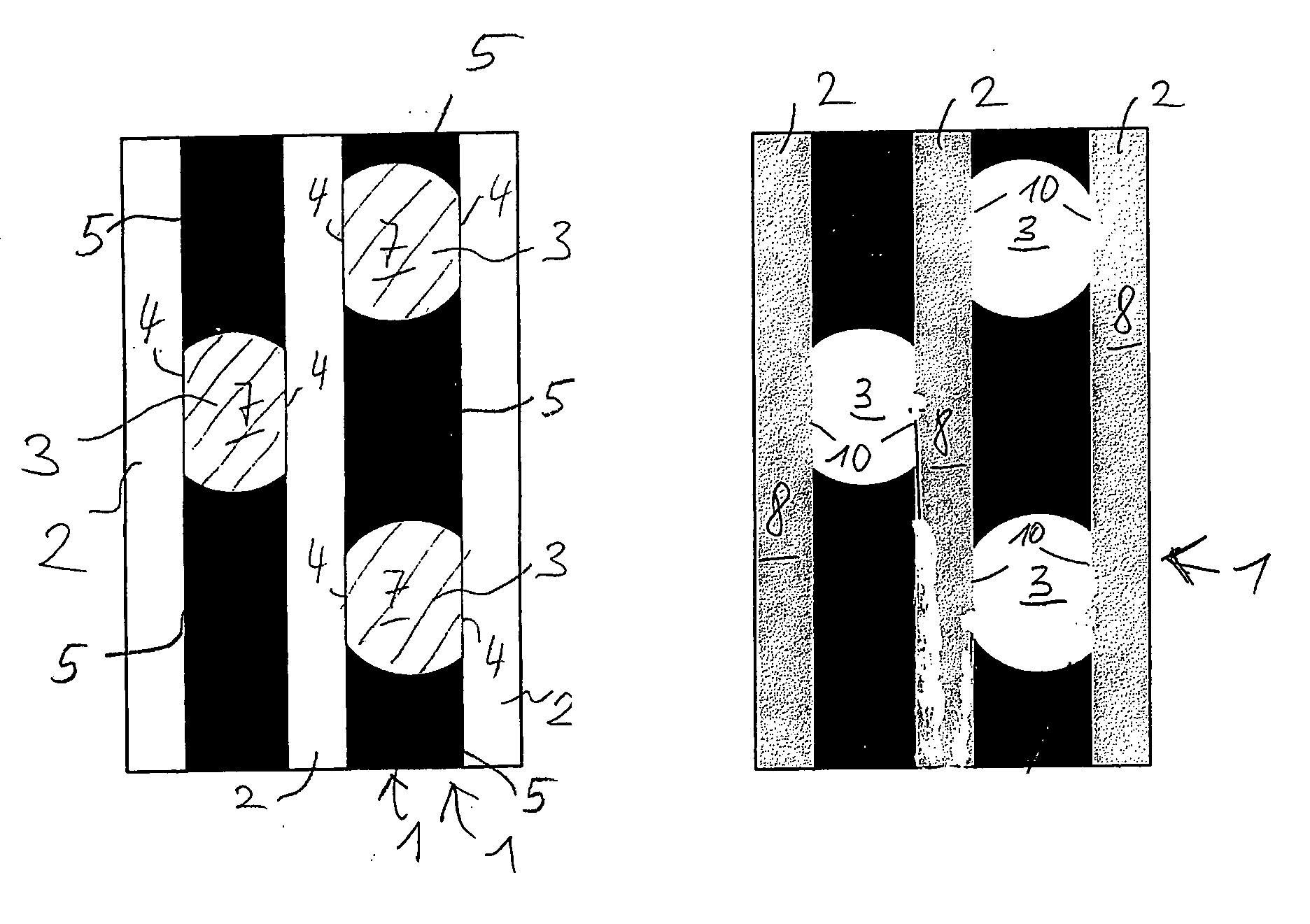
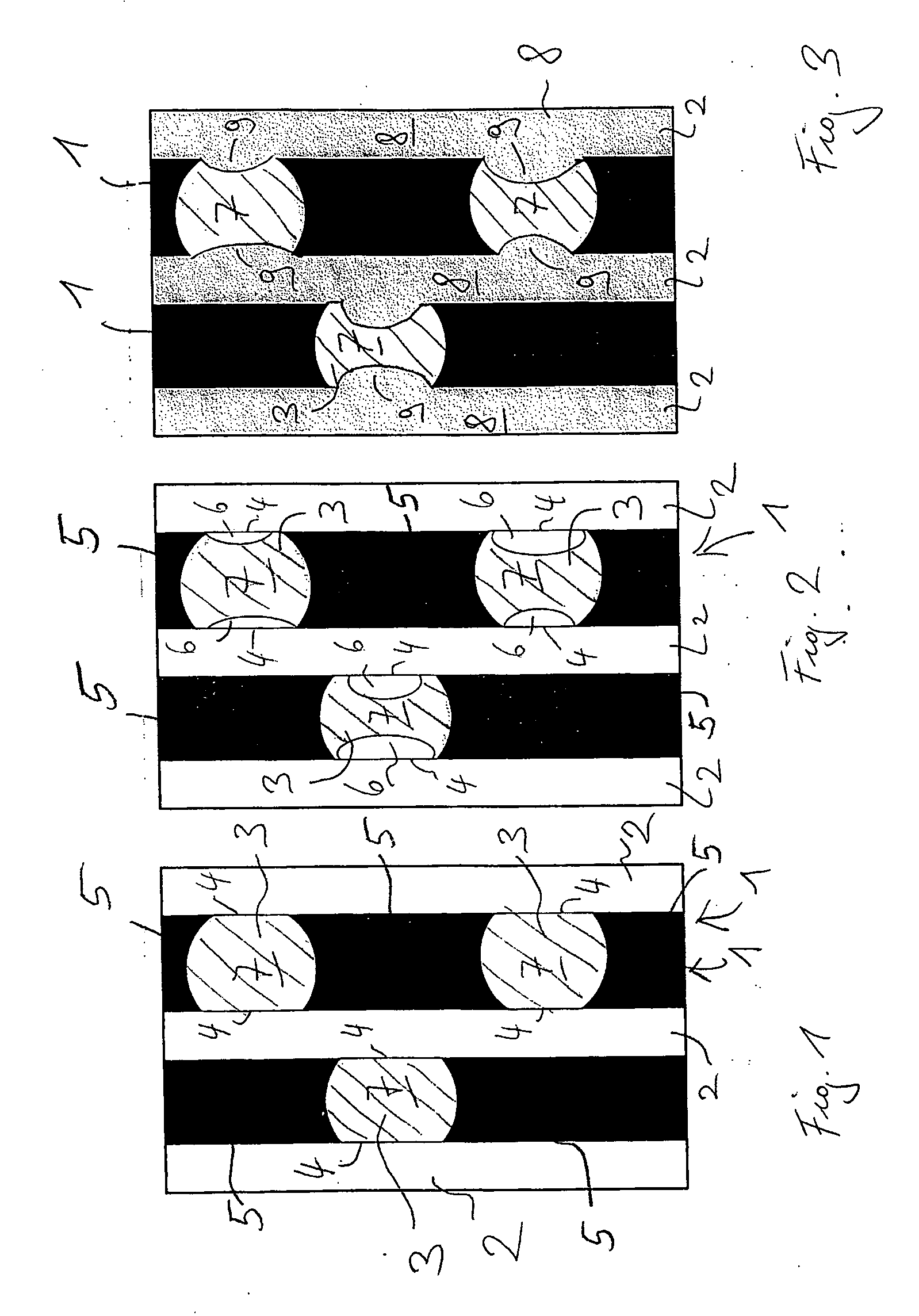
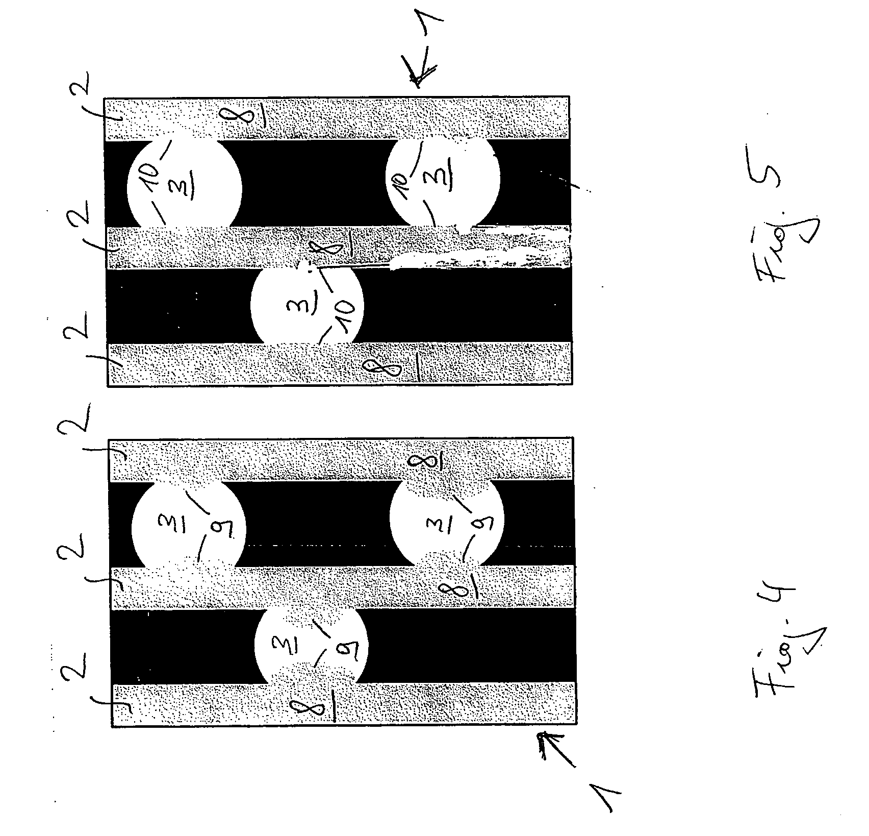
[0037] The invention may be used in any technical field using dielectric material. The invention is useful for producing isolating trenches with high aspect ratios, e.g. for producing isolating trenches for semiconductor devices. The inventive methods may be used for producing isolating trenches for three-dimensional electronic devices, e.g. FIN-FET. Additionally, the inventive method may be used in CMOS processes and by producing memory devices, e.g. DRAM memories or logic devices.

[0038] The invention is described considering a DRAM memory and a method for producing a DRAM memory as example. However, the use of the inventive method is not restricted to this example. A DRAM memory comprises memory cells with transistors and a data storing elements, e.g. a trench capacitor. The storing element is produced in a semiconductor substrate 1. The semiconductor substrate 1 is usually formed of a silicon wafer. On an upper surface of the substrate 1, trenches 2 are formed. These trenches ma...


PUM

PropertyMeasurementUnit
temperatureaaaaaaaaaa

Abstract

The present invention relates to a method of forming an isolating trench of a semiconductor device with a dielectric material, and to a method of forming an isolating trench in a memory device.

Description

TECHNICAL FIELD OF THE INVENTION [0001] The present invention relates to a method of forming an isolating trench of a semiconductor device with a dielectric material, and to a method of forming an isolating trench in a memory device. BACKGROUND OF THE INVENTION [0002] As ground rule dimensions shrink in integrated circuits, the problem of filling high aspect ratio trenches increases, in particular for isolation trenches used in shallow trench isolation processes, STI, which is commonly used in advanced processing. [0003] Furthermore, with higher aspect ratios it becomes increasingly difficult to fill trenches with dielectric material free of voids and gaps. A possibility to overcome this problem is to use spin-on dielectric materials in order to fill the trenches. However, spin-on dielectric materials or spin-on glass have to subjected to a densification and / or curing process. The densification process is necessary in order to obtain e.g. a low wet etch rate for further wet etch pro...

Claims


Application Information

Patent Timeline
Patent Type & Authority Applications(United States)
IPC IPC(8): H01L21/76
CPCH01L21/76224H01L27/10826H01L27/10844H01L29/785H10B12/36H10B12/01
Inventor WELLHAUSEN, UWEHEIDEMEYER, HENRYREGUL, JOERN
Owner POLARIS INNOVATIONS LTD
Why Eureka
Try Eureka