Serial flash semiconductor memory

a semiconductor memory and serial flash technology, applied in the field of flash semiconductor memory, can solve the problems of increasing density requirements, serial flash tends to consume less power, and the overhead of most application specific controllers, and achieves the effects of improving performance and features, reducing pin counts, and accelerating transfer rates and code execution capabilities

Active Publication Date: 2009-07-07
WINBOND ELECTRONICS CORP
View PDF20 Cites 118 Cited by
  • Summary
  • Abstract
  • Description
  • Claims
  • Application Information

AI Technical Summary

Benefits of technology

[0021]The present invention advantageously offers the low pin-count and space-efficient packaging of conventional serial flash memory with faster transfer rates and code execution capability which in some embodiments approaches that of parallel flash, even while supporting conventional serial flash interfaces. These enhanced capabilities allow for increased performance and features as needed in the application.

Problems solved by technology

This is a considerable overhead for most application specific controllers.
Additionally, serial flash tends to consume less power during read than parallel flash.
While this may be acceptable for lower density serial flash of less than 4 M-bit, for example, the power-up delay can increase as density requirements increase.
Code execution on a serial flash memory is not practical because of the amount of overhead required.
The overhead of a serial flash is further increased when the instruction sequence encounters frequent address jumps or calls, each of which would require another serial read instruction to be shifted in bit-by-bit.
However, the clock frequency is reduced by 75% when using the parallel interface, substantially limiting the net gain in transfer rate.

Method used


Image

  • Serial flash semiconductor memory
  • Serial flash semiconductor memory
  • Serial flash semiconductor memory

Examples


example b

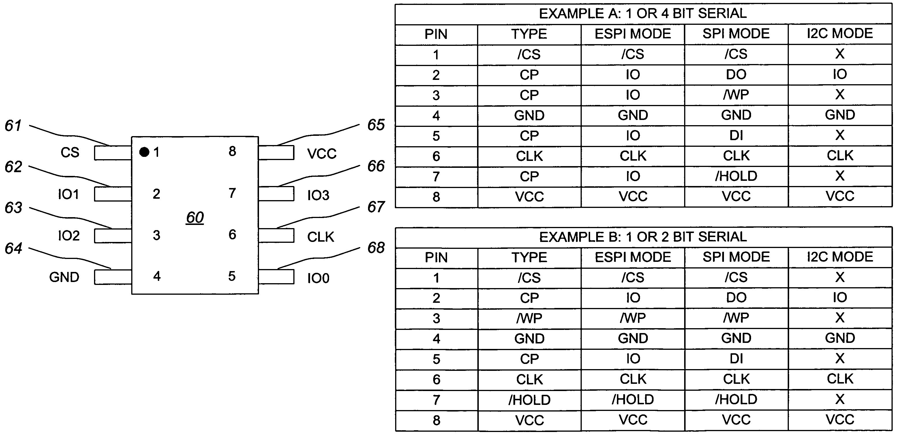
[0060]In Example B, one of the pins is a data output pin and the other three pins are IO pins. In ESPI mode, one of the IO pins is used as a data input pin and the remaining two other pins are used as data IO pins so that three bits may be input using the IO pins and three bits may be output using the DO pin and two of the IO pins. In SPI mode, one IO pin is used as a data input pin. In I2C mode, one of the IO pins is used as a data IO pin.

[0061]In Example C, one of the pins is a data input pin and the other three pins are IO pins. In ESPI mode, one of the IO pins is used as a data output pin and the remaining two other pins are used as data IO pins so that three bits may be output using the IO pins and three bits may be input using the DI pin and two of the IO pins. In SPI mode, one IO pin is used as a data output pin. In I2C mode, one of the IO pins is used as a data IO pin.

[0062]In Example D of FIG. 8, one pin is a data input pin, one pin is a data output pin, and the other two p...


PUM


Abstract

A serial flash memory is provided with multiple configurable pins, at least one of which is selectively configurable for use in either single-bit serial data transfers or multiple-bit serial data transfers. In single-bit serial mode, data transfer is bit-by-bit through a pin. In multiple-bit serial mode, a number of sequential bits are transferred at a time through respective pins. The serial flash memory may have 16 or fewer pins, and even 8 or fewer pins, so that low pin count packaging such as the 8-pin or 16-pin SOIC package and the 8-contact MLP / QFN / SON package may be used. The availability of the single-bit serial type protocol enables compatibility with a number of existing systems, while the availability of the multiple-bit serial type protocol enables the serial flash memory to provide data transfer rates, in systems that can support them, that are significantly faster than available with standard serial flash memories.

Description

CROSS-REFERENCE TO RELATED APPLICATIONS[0001]This patent is a continuation-in-part of and claims the benefit of U.S. patent application Ser. No. 10 / 951,187 filed Sep. 27, 2004 now abandoned (Jigour et al., “Serial flash semiconductor memory”), which hereby is incorporated herein in its entirety by reference thereto.STATEMENT REGARDING FEDERALLY SPONSORED RESEARCH OR DEVELOPMENT[0002]Not ApplicableBACKGROUND OF THE INVENTION[0003]1. Field of the Invention[0004]The present invention relates to flash semiconductor memory, and more particularly to serial flash semiconductor memory.[0005]2. Description of the Related Art[0006]Electronic systems have traditionally used parallel “NOR” flash memories for non-volatile code storage, and in some cases data storage. Newer serial flash memories, with their low pin-count and small packaging, are an alternative to ordinary parallel flash memories for code and data storage requirements. As a result, the use of serial flash memory is gaining momentu...

Claims


Application Information

Patent Timeline
Patent Type & Authority Patents(United States)
IPC IPC(8): G06F13/14G06F13/42G06F3/00
CPCG11C7/1045G11C8/04G11C16/26G11C2216/30G11C2207/108
Inventor JIGOUR, ROBIN J.PARK, EUNGJOONPARK, JOO WEONLEE, JONG SEUK
Owner WINBOND ELECTRONICS CORP
Why Eureka
Try Eureka