Semiconductor device

a technology of semiconductor elements and semiconductor devices, which is applied in the direction of semiconductor devices, digital storage, instruments, etc., can solve the problems of difficult minute control of electric charge amount, increase in circuit size, and limitation of electric charge holding capacity, so as to achieve easy control of potential of nodes, easy storage, and constant or substantially constant potential of nodes

Active Publication Date: 2013-11-12
SEMICON ENERGY LAB CO LTD
View PDF160 Cites 22 Cited by
  • Summary
  • Abstract
  • Description
  • Claims
  • Application Information

AI Technical Summary

Benefits of technology

[0022]A semiconductor device according to an embodiment of the present invention includes a memory cell which holds data in a node to which one of a source and a drain of a transistor whose channel region is formed from an oxide semiconductor is electrically connected. Note that the value of off-state current (leakage current) of the transistor is extremely small. Thus, after being set to have a predetermined value, the potential of the node can be kept constant or substantially constant by turning the transistor off. In this manner, accurate data can be stored in the memory cell.
[0023]The node is electrically connected to the one of the source and the drain of the transistor. Thus, the potential of the node can be easily controlled by transfer of electric charge through the transistor. In other words, multilevel data can be easily stored in the memory cell.
[0024]As compared to the flash memories, in the semiconductor device according to an embodiment of the present invention, data stored in the node is less affected by a specific semiconductor element. In other words, the memory cell can store data without being greatly influenced by variation in the characteristics of semiconductor elements. Thus, potentials can take a plurality of values with short intervals and held in the node as data.
[0025]In the semiconductor device according to an embodiment of the present invention, a row address signal and a column address signal are supplied through one wiring. Thus, the number of pins in the semiconductor device can be reduced.

Problems solved by technology

An increase in storage capacity causes an increase in circuit size.
However, there is limitation on the amount of electric charge which can be held in the floating gate and the amount of electric charge is difficult to minutely control.
Thus, when multilevel data is stored in a memory cell, probability of failure of retention of accurate data becomes higher.

Method used


Image

  • Semiconductor device
  • Semiconductor device
  • Semiconductor device

Examples


Embodiment Construction

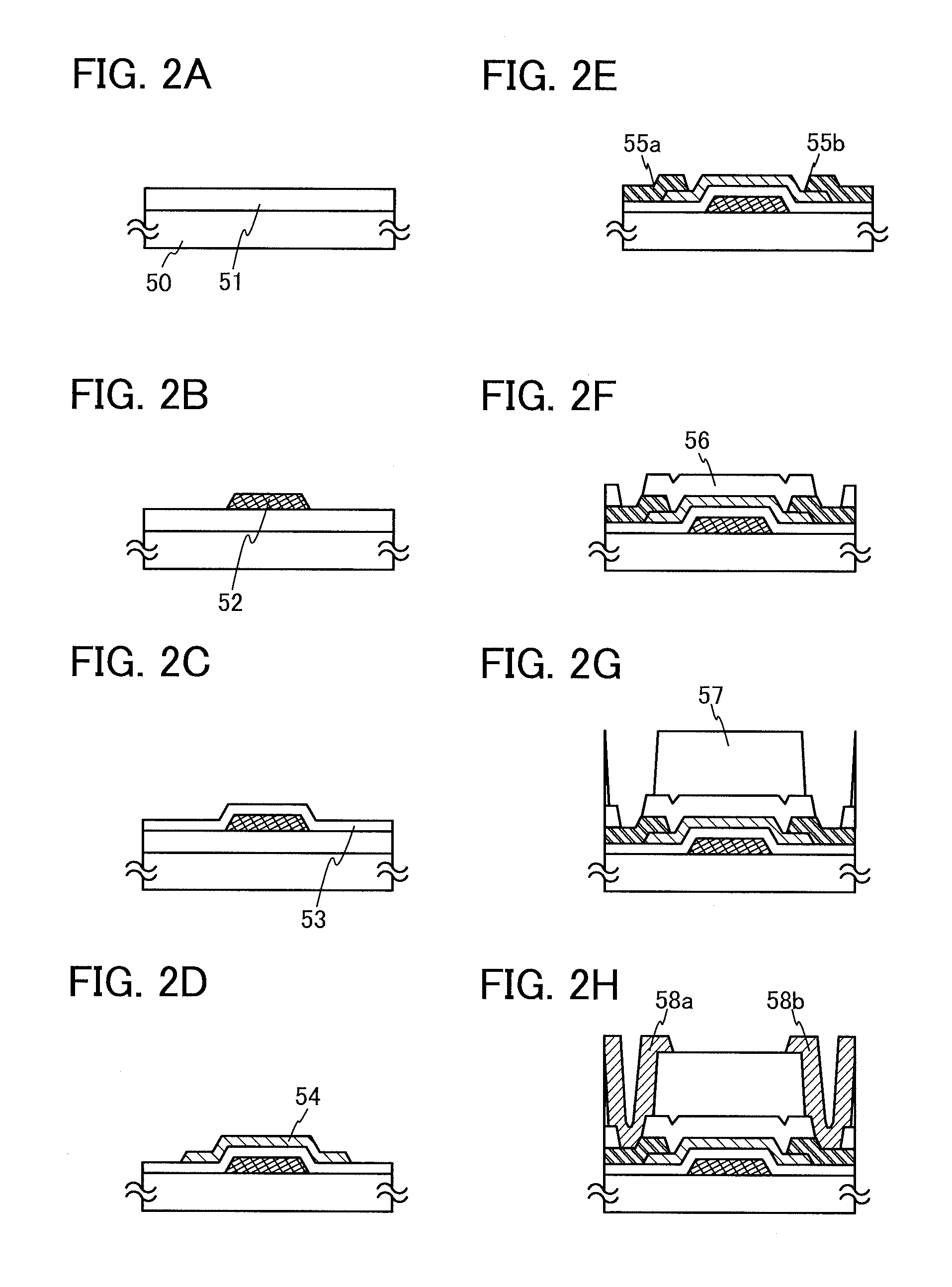
[0052]An embodiment of the present invention will be described below in detail with reference to the drawings Note that the present invention is not limited to the following description. It will be readily appreciated by those skilled in the art that modes and details of the present invention can be changed in various ways without departing from the spirit and scope of the present invention. Thus, the present invention should not be construed as being limited to the following description of the embodiment.

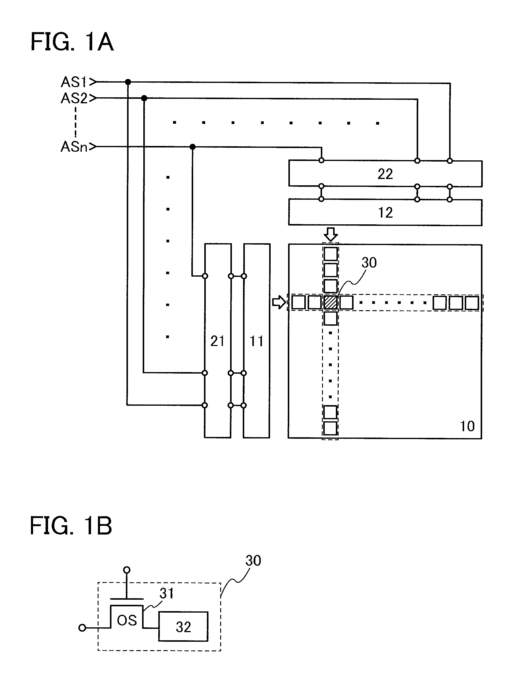
[0053]First, a semiconductor device according to an embodiment of the present invention is described with reference to FIGS. 1A and 1B.

[0054]FIG. 1A illustrates a structure example of a semiconductor device according to an embodiment of the present invention. The semiconductor device illustrated in FIG. 1A includes the following components: a memory cell array 10 including a plurality of memory cells 30 arranged in matrix; a row decoder 11 which selects a given row of the memory ce...


PUM


Abstract

An object is to provide a semiconductor device which includes a memory cell capable of holding accurate data even when the data is multilevel data. The semiconductor device includes a memory cell holding data in a node to which one of a source and a drain of a transistor whose channel region is formed from an oxide semiconductor. Note that the value of off-state current (leakage current) of the transistor is extremely small. Thus, after being set to have a predetermined value, the potential of the node can be kept constant or substantially constant by turning the transistor off. In this manner, accurate data can be stored in the memory cell.

Description

BACKGROUND OF THE INVENTION[0001]1. Field of the Invention[0002]The present invention relates to a semiconductor device using a semiconductor element. In particular, the present invention relates to a semiconductor device including a memory device using a semiconductor element. Note that the semiconductor device in this specification indicates all the devices that operate by utilizing semiconductor characteristics.[0003]2. Description of the Related Art[0004]Memory devices using semiconductor elements are broadly classified into two categories: a volatile device that loses stored data when power supply stops, and a non-volatile device that retains stored data even when power is not supplied.[0005]A typical example of a volatile memory device is a DRAM (dynamic random access memory). A DRAM stores data in such a manner that a transistor included in a memory cell is selected and electric charge is stored in a capacitor.[0006]When data is read from a DRAM, electric charge in a capacito...

Claims


Application Information

Patent Timeline
Patent Type & Authority Patents(United States)
IPC IPC(8): G11C11/24
CPCG11C16/0433G11C16/08H01L27/11517H01L27/1225G11C11/403G11C11/565G11C11/5685G11C13/0004G11C13/003H10B41/00H10B99/00H10B12/00
Inventor YAMAZAKI, SHUNPEIKOYAMA, JUN
Owner SEMICON ENERGY LAB CO LTD
Why Eureka
Try Eureka