Anti-electrostatic substrate
An anti-static, substrate technology, applied in the direction of static electricity, circuit substrate materials, electric light sources, etc., can solve the problems of process pass rate decline, achieve the effect of improving pass rate and eliminating static damage phenomenon
- Summary
- Abstract
- Description
- Claims
- Application Information
AI Technical Summary
Problems solved by technology
Method used
Image

Examples
Embodiment Construction
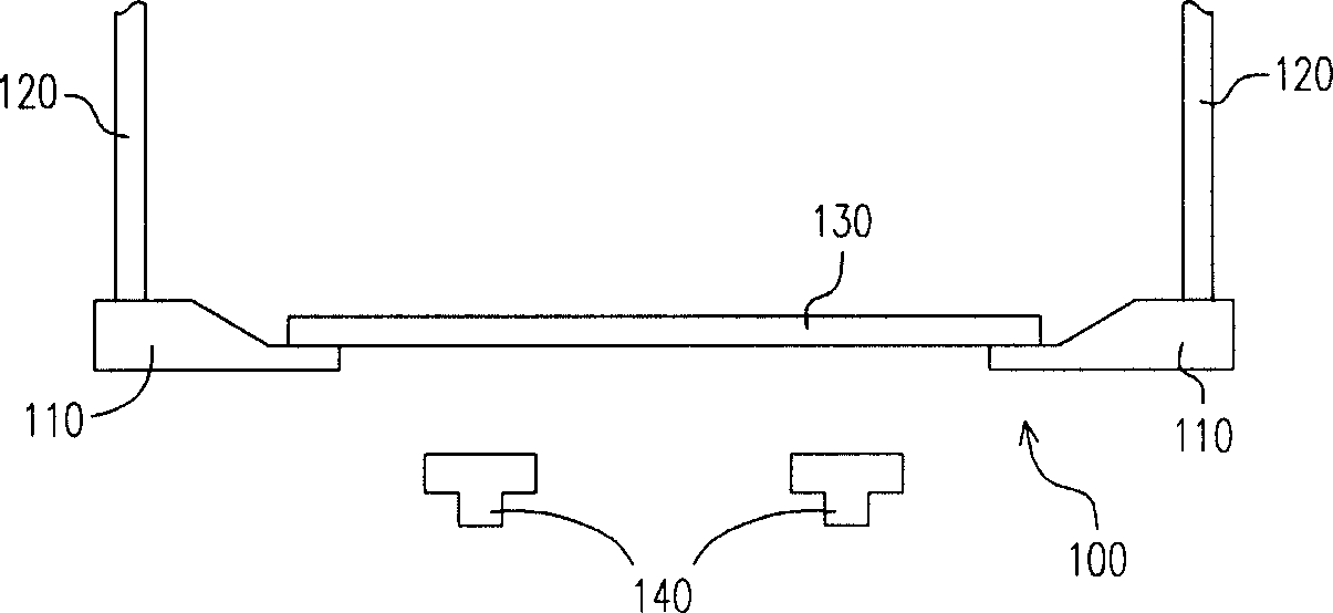
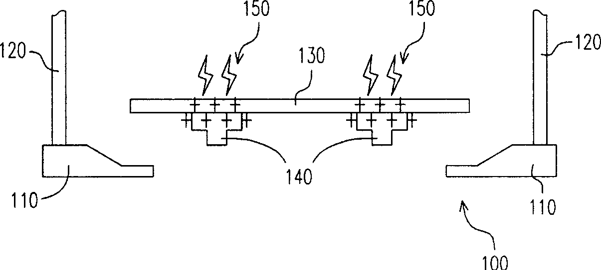
[0037] Fig. 3 is a schematic diagram of an antistatic substrate in a preferred embodiment of the present invention. FIG. 4 is a schematic diagram of using a conveying device to convey the antistatic substrate in FIG. 3 in the present invention. Please refer to FIG. 3 and FIG. 4 together. The antistatic substrate 200 is suitable for eliminating the static electricity 230 generated by friction between the transport device 100 and the antistatic substrate 200 . The conveying device 100 is the same or similar to the conveying device 100 shown in FIG. 2 , so details are not repeated here.
[0038] Please refer to FIG. 3 , the antistatic substrate 200 includes a substrate 210 and a conductive film 220 . The substrate 210 has a front surface 212 and a back surface 214 , and the conductive film 220 is disposed on the back surface 214 . Please refer to FIG. 4 again. When the transport device 100 (ie, the robot arm 140 in FIG. 4 ) contacts the conductive film 220, the static electrici...
PUM
 Abstract
Description
Claims
Application Information
 - R&D Engineer
- R&D Manager
- IP Professional
- Industry Leading Data Capabilities
- Powerful AI technology
- Patent DNA Extraction
Browse by: Latest US Patents, China's latest patents, Technical Efficacy Thesaurus, Application Domain, Technology Topic.
© 2024 PatSnap. All rights reserved.Legal|Privacy policy|Modern Slavery Act Transparency Statement|Sitemap