Method and system for testing chip

A chip to be tested, chip technology, applied in the field of testing, can solve problems such as difficult comparison

Inactive Publication Date: 2007-03-07
GUANGDONG BOGUAN TECH
View PDF0 Cites 15 Cited by
  • Summary
  • Abstract
  • Description
  • Claims
  • Application Information

AI Technical Summary

Problems solved by technology

Therefore, it is very difficult to compare the resu

Method used


Image

  • Method and system for testing chip
  • Method and system for testing chip
  • Method and system for testing chip

Examples


Embodiment Construction

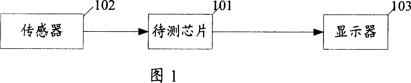
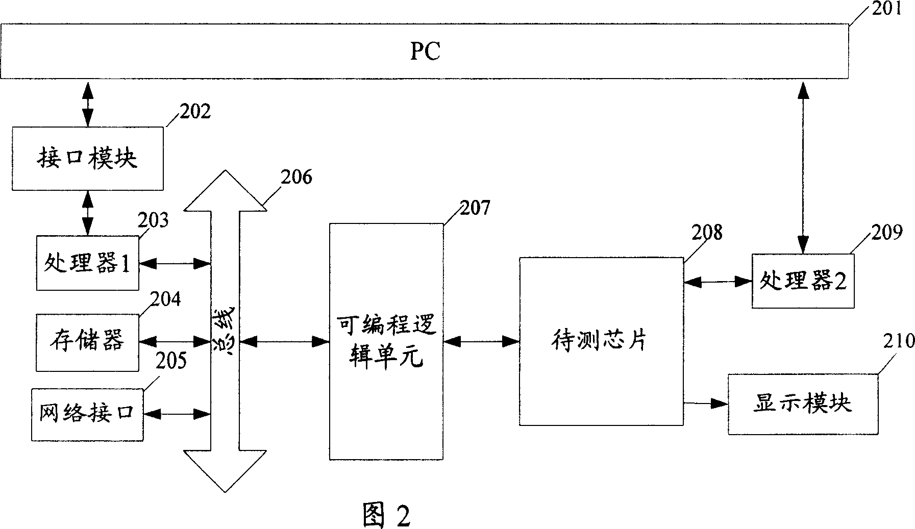
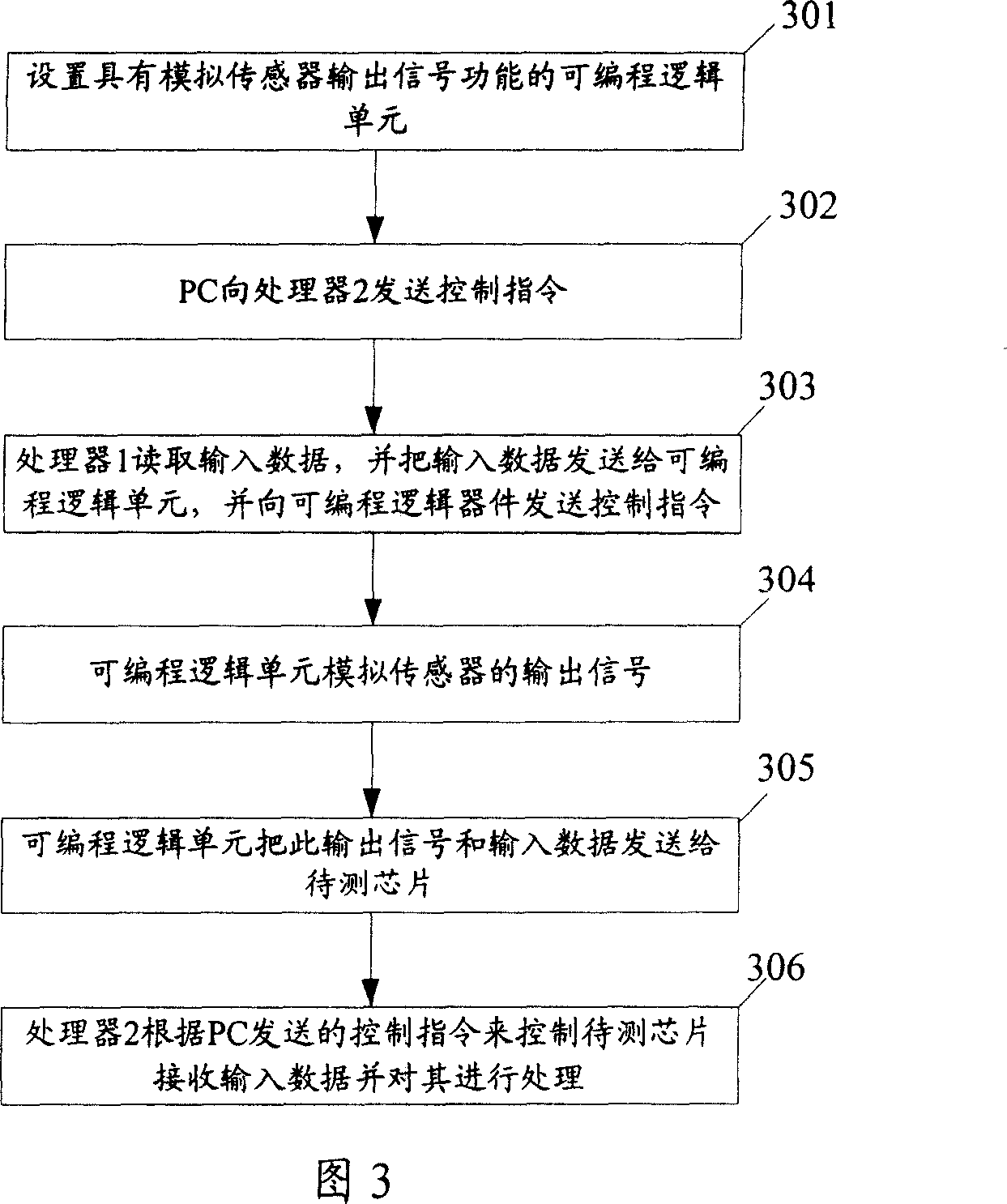
[0051] Firstly, the general inventive idea of ​​a chip testing system of the present invention is introduced.

[0052] As shown in Figure 2, the system of a kind of test chip of the present invention comprises PC201, interface module 202, processor 1203, memory 204, network interface 205, bus 206, programmable logic unit 207, chip to be tested 208, processor 2209 and display module 210 .

[0053] The PC 201 sends a control command to the processor 1203 through the interface module 202, and the processor 1203 reads the input data on the memory 204 through the bus 206 according to the control command, and the processor 1203 sends the input data to the programmable logic unit 207 through the bus 206, and Send the control instruction to the programmable logic unit 207, and the programmable logic unit 207 simulates the output signal of the sensor according to the control instruction, and sends the output signal and input data to the chip 208 under test. PC201 sends a control instruc...


PUM


Abstract

This invention discloses one test chip method, which comprises the following steps: a, setting programmable logic unit with analogue sensor output signals; b, programmable logic unit receiving input data and analogue output signal of sensor and the unit inputs the signals to the chip tested; c, receiving input data by use of output signal for data process. This invention compares the results of chips and software evaluation tool and also compares the chip and input data to observe chip computation formula effect.

Description

technical field [0001] The invention relates to a test technology, in particular to a method and system for testing a chip. Background technique [0002] In the process of chip development and manufacturing, the process of testing the chip must be carried out. As shown in Figure 1, it is a schematic diagram of the composition and structure of the system that needs to be built for the prior art test chip, which includes: [0003] Sensor 102: used to collect input data that needs to be processed and output the output as the input of the chip to be tested. [0004] The chip under test 101 is used to process the output of the sensor 102 and send the processing result to the display 103 . Different chips have different processing functions. For example, the image processing chip in the multimedia processing chip has the functions of image gain control, image format conversion, image scaling, color adjustment and gamma correction; the sound processing chip has the function of so...

Claims


Application Information

Patent Timeline
IPC IPC(8): G06F11/267
Inventor 黄鑫游明琦
Owner GUANGDONG BOGUAN TECH
Why Eureka
Try Eureka