Organic electroluminescent device, method of manufacturing organic electroluminescent device, and electronic apparatus

An electroluminescent device and manufacturing method technology, applied in the direction of electroluminescent light source, electric light source, lighting device, etc., can solve the problems of display image color temperature drop, display quality reduction, display quality damage, etc., to achieve the suppression of color shift or the effect of reducing the brightness

Inactive Publication Date: 2007-03-14
SEIKO EPSON CORP
View PDF2 Cites 9 Cited by
  • Summary
  • Abstract
  • Description
  • Claims
  • Application Information

AI Technical Summary

Problems solved by technology

In particular, since green is highly visible, it becomes an easily recognizable color shift, resulting in a decrease in display quality
[0015] Moreover, when blue and green have the above-mentioned

Method used


Image

  • Organic electroluminescent device, method of manufacturing organic electroluminescent device, and electronic apparatus
  • Organic electroluminescent device, method of manufacturing organic electroluminescent device, and electronic apparatus
  • Organic electroluminescent device, method of manufacturing organic electroluminescent device, and electronic apparatus

Examples


Embodiment Construction

[0058] Hereinafter, the present invention will be described in detail.

[0059] In addition, this embodiment represents a part of the aspect of the present invention, and does not limit the present invention, and can be changed arbitrarily within the scope of the technical idea of ​​the present invention. In addition, in each of the drawings shown below, since each layer and each member are formed in a size that is recognizable on the drawing surface, different scales are adopted for each layer and each member.

[0060] (Organic EL Panel)

[0061] First, an embodiment with an EL panel of the organic EL device of the present invention will be described.

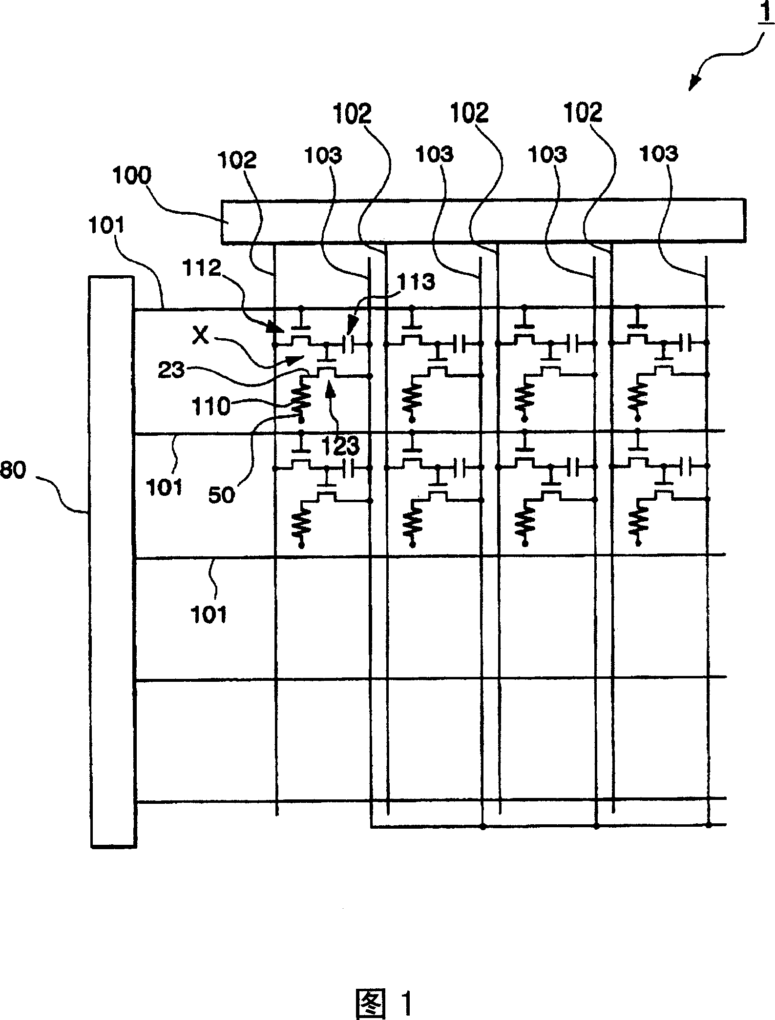
[0062] FIG. 1 is a schematic diagram showing the wiring structure of the organic EL panel 1.

[0063] The organic EL panel 1 of the present embodiment is an active matrix type panel using thin film transistors (Thin Film Transistor, hereinafter referred to as TFT.) as switching elements, and has a plurality of scanning lines 101.....


PUM


Abstract

The invention provides an organic EL (ElectroLuminescent) device, a method of manufacturing an organic EL device, and an electronic apparatus free from color shift or change of brightness even when an observer sees it from front or at wide angles. Of the organic electroluminescent device 1A equipped with pixels XB, XG, XR each having a light-emitting function layer pinched by a first electrode 23 and a second electrode 50, and a unit pixel group Px consisting of a plurality of pixels XB, XG, XR, selected pixels out of the unit pixel group Px are provided with a dispersion part 21 for dispersing emission light L of the light-emitting function layer 110.

Description

Technical field [0001] The present invention relates to an organic electroluminescence device, a manufacturing method of the organic electroluminescence device, and electronic equipment. Background technique [0002] As a display device used in electronic devices such as mobile phones, personal computers or PDAs (Personal Digital Assistants), or exposure heads in image forming devices such as digital copiers or printers, organic electroluminescent devices (hereinafter, It is called organic EL device.) and other light-emitting devices are attracting attention. When such a light-emitting device is called a color light-emitting device, conventionally, by changing the material constituting the light-emitting layer for each pixel, light of various colors is emitted from each pixel. [0003] In addition, in recent years, there has been proposed a structure in which a sacrificial oxide film is formed on the glass substrate of an organic EL device to prevent light from being trapped in t...

Claims


Application Information

Patent Timeline
IPC IPC(8): H05B33/00H05B33/22H05B33/10
CPCH01L27/322H01J1/70H01L51/5268H01J1/74H01L27/3211H01L51/5237H01J29/325H10K59/35H10K59/38H10K50/854H10K50/844H05B33/22
Inventor 和野裕美
Owner SEIKO EPSON CORP
Why Eureka
Try Eureka