Top-emission active matrix electroluminecient device

Active Publication Date: 2009-06-11
INNOLUX CORP
View PDF5 Cites 4 Cited by
  • Summary
  • Abstract
  • Description
  • Claims
  • Application Information

AI Technical Summary

Benefits of technology

[0009]The alternative top-emission active matrix electroluminecient device also comprises a passivation layer which is under the first reflective layer region and which covers the second reflective layer region and the third reflective layer region. An insulating layer is further provided between the second reflective layer region and

Problems solved by technology

On one hand, the micro-cavity effect improves emission luminance of the conventional electroluminecient device, and on the other hand

Method used


Image

  • Top-emission active matrix electroluminecient device
  • Top-emission active matrix electroluminecient device
  • Top-emission active matrix electroluminecient device

Examples


Example

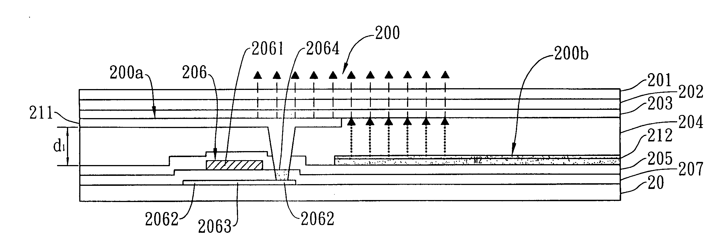
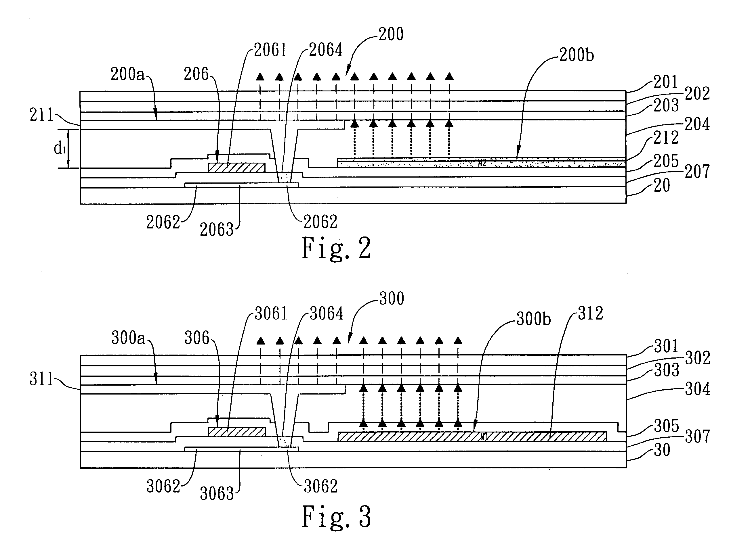
[0019]In the first embodiment, part of the light from the electroluminecient layer 202 emits toward the first reflective layer region 200a and the second reflective layer region 200b, through both of which the part of the light is reflected and returns to the region between the first conductive electrode layer 201 and the second conductive electrode layer 203. Then, said part of the light may be emitted directly out of the top of the electroluminecient device 200; otherwise, it may be emitted out of the top of the electroluminecient device 200 after a micro-cavity effect occurs within the region between the first conductive electrode layer 201 and the second conductive electrode layer 203. As shown in FIG. 2, the optical path length of the light reflected from the first reflective layer region 200a is different from that of the light reflected from the second reflective layer region 200b. Consequently, when the light reflected respectively from the first reflective layer region 200a...

Example

[0022]In the second embodiment, part of the light from the electroluminecient layer 302 emits toward the first reflective layer region 300a and the second reflective layer region 300b, through both of which the part of the light is reflected and returns to the region between the first conductive electrode layer 301 and the second conductive electrode layer 303. Then, the part of the light may be emitted directly out of the top of the electroluminecient device 300; otherwise, it may be emitted out of the top of the electroluminecient device 300 after a micro-cavity effect occurs within the region between the first conductive electrode layer 301 and the second conductive electrode layer 303. As shown in FIG. 3, the light reflected from the first reflective layer region 300a has an optical path length different from that of the light reflected from the second reflective layer region 300b. Consequently, when the light reflected respectively from the first reflective layer region 300a an...

Example

[0025]In the third embodiment, part of the light from the electroluminecient layer 402 emits toward the first reflective layer region 400a, the second reflective layer region 400b and the third reflective layer region 400c, through all of which the part of the light is reflected and returns to the region between the first conductive electrode layer 401 and the second conductive electrode layer 403. Then, the part of the light may be emitted directly out of the top of the electroluminecient device 400; otherwise, it may be emitted out of the top of the electroluminecient device 400 after a micro-cavity effect occurs within the region between the first conductive electrode layer 401 and the second conductive electrode layer 403. As shown in FIG. 4, the light reflected from the first reflective layer region 400a has an optical path length different from that of the light reflected from the second reflective layer region 400b and different from that of the light reflected from the third...


PUM


Abstract

This invention provides a top-emission active matrix electroluminecient device including a substrate and a plurality of pixel areas formed within a display area of the substrate. Each of the pixel areas includes at least one sub-pixel area comprising at least, from top to bottom: a first conductive electrode layer, an electroluminecient layer, a second conductive electrode layer, a first reflective layer region, and a second reflective layer region. The first reflective layer region and second reflective layer region overlap each other in part. Some of the light rays emitted from the electroluminecient layer are reflected by the first reflective layer region and second reflective layer region, respectively, and are then directed upwards. The reflected light rays compensate the top-emitting light rays also emitted from the electroluminecient layer, reducing color shifts at different viewing angles due to the micro-cavity effect.

Description

BACKGROUND OF THE INVENTION[0001]1. Field of the Invention[0002]The present invention relates to an active matrix electroluminecient device, and more particularly, to a top-emission active matrix electroluminecient device.[0003]2. Description of the Related Art[0004]Electroluminecient display devices are active display devices that have many advantages over cathode-ray tubes (CRTs) or liquid crystal displays (LCDs). For example, an electroluminecient display device typically has a wide viewing angle, high brightness and contrast, high response speed, light weight, small size, thin thickness, and low power consumption. FIG. 1A is a schematic cross-sectional view showing the partial structure of a conventional top-emission active matrix electroluminecient device corresponding to a pixel area. The conventional electroluminecient device mainly comprises, from top to bottom: a transparent cathode layer 101, an electroluminecient layer 102, a transparent anode layer 103, a metallic reflec...

Claims


Application Information

Patent Timeline
IPC IPC(8): H01J1/63
CPCH01L51/5265H01L27/12H10K50/852
Inventor CHAN, CHUAN-YIPENG, DU-ZENRYUJI, NISHIKAWA
Owner INNOLUX CORP
Why Eureka
Try Eureka