Lithographic apparatus, device manufacturing method and device manufactured thereby

A lithography and fixture technology, which can be used in semiconductor/solid-state device manufacturing, photolithography process exposure devices, microlithography exposure equipment, etc., and can solve problems such as pattern formation and structure distortion

Active Publication Date: 2007-04-04
ASML NETHERLANDS BV +1
View PDF1 Cites 19 Cited by
  • Summary
  • Abstract
  • Description
  • Claims
  • Application Information

AI Technical Summary

Problems solved by technology

Creates a temperature offset between the patterning structure and the patterning structure fixture that can cause distortion of the patterning structure, strain in the patterning structure and overlay errors

Method used


Image

  • Lithographic apparatus, device manufacturing method and device manufactured thereby
  • Lithographic apparatus, device manufacturing method and device manufactured thereby
  • Lithographic apparatus, device manufacturing method and device manufactured thereby

Examples


Embodiment Construction

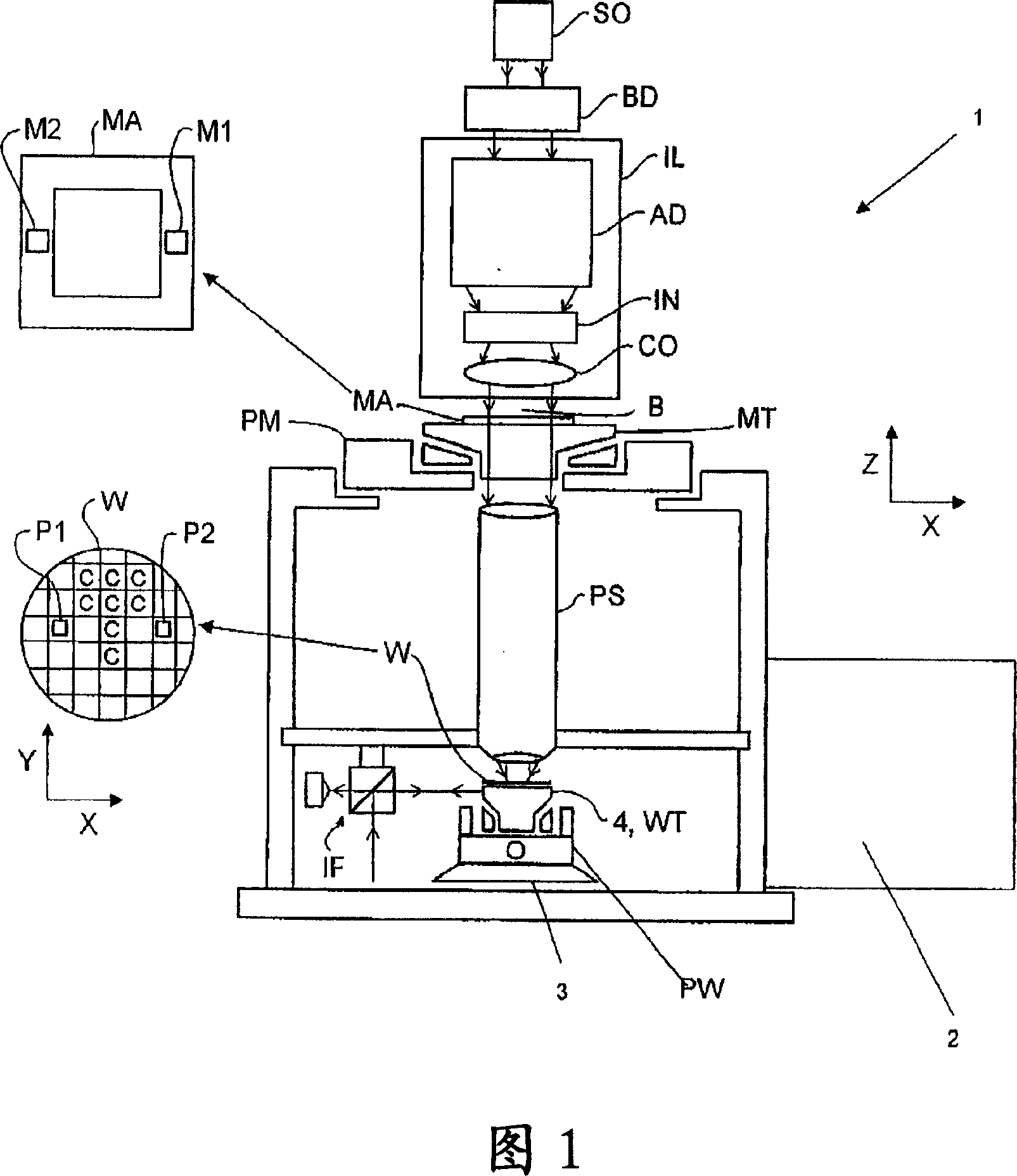
[0031] Fig. 1 schematically shows a lithographic apparatus 1 according to an embodiment of the present invention. The device 1 may include:

[0032] an illumination system (illuminator) IL configured to adjust a radiation beam B (eg UV radiation or another type of radiation);

[0033] a support structure (eg, mask table) MT configured to support the patterning structure (eg, mask) MA, connected to a first positioning device PM configured to accurately position the patterning structure according to certain parameters;

[0034] A substrate stage 3 having a substrate holding device, which may include a chuck 4 with a substrate table (e.g., a wafer table) WT configured to hold a substrate (e.g., coated with a etchant wafer) W and is connected to a second positioning device PW configured to accurately position the substrate according to certain parameters;

[0035] a projection system (e.g. a refractive type projection lens system) PL configured to project the pattern imparted by...


PUM


Abstract

A lithographic apparatus configured to transfer a pattern from a patterning structure to a substrate is disclosed, comprising a substrate holder configured to hold a substrate and a substrate configured to transfer the substrate to the substrate holder. A substrate temperature regulator that adjusts the temperature of the substrate to substantially match the temperature of the substrate holder before, during, or both. Further provided is a lithographic apparatus configured to transfer a pattern from a patterned structure onto a substrate, comprising a first patterning structure holding device configured to hold the patterned structure; A pattern forming structure temperature adjusting device for adjusting the temperature of the pattern forming structure before being transferred to the pattern forming structure holding device, wherein the pattern forming structure temperature adjusting device is provided with a second pattern forming structure holding device; and at least one for applying the first and the second A system in which two patterning structure fixtures are thermally conditioned to approximately the same temperature.

Description

technical field [0001] The present invention relates to a photolithography apparatus, a device manufacturing method and devices manufactured therefrom. Background technique [0002] A lithographic apparatus is a machine that can apply a desired pattern on a substrate, usually a target portion of the substrate. A lithographic apparatus may be used, for example, in the manufacture of integrated circuits (ICs). In this case, a patterning structure, also known as a mask or reticle, may be employed to create the circuit pattern to be formed on the individual layers of the IC. The pattern can be transferred to a target portion (eg, comprising one or more dies) on a substrate (eg, a silicon wafer). Transfer of the pattern is usually accomplished by means of imaging onto a layer of radiation-sensitive material (resist) provided on the substrate. Typically, a single substrate contains a network of adjacent target portions that are successively patterned. Known lithographic appara...

Claims


Application Information

Patent Timeline
Patent Type & Authority Applications(China)
IPC IPC(8): G03F7/20H01L21/027
CPCG03F7/70741G03F7/70875G03F7/7075
Inventor J·J·奎特P·沙普S·罗克斯G·奥康纳
Owner ASML NETHERLANDS BV
Why Eureka
Try Eureka