Pattern density control method using edge printing processes
A manufacturing method and process technology, applied in the field of pattern density control, can solve problems such as changes in polishing and internal etching steps, etc.
- Summary
- Abstract
- Description
- Claims
- Application Information
AI Technical Summary
Problems solved by technology
Method used
Image

Examples
Embodiment Construction
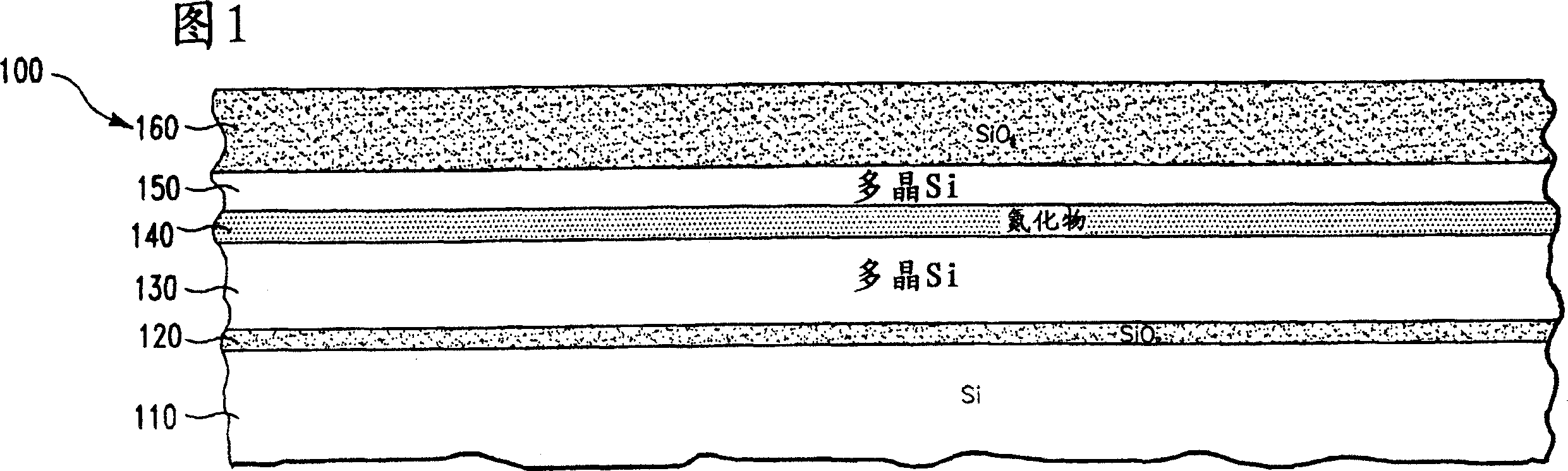
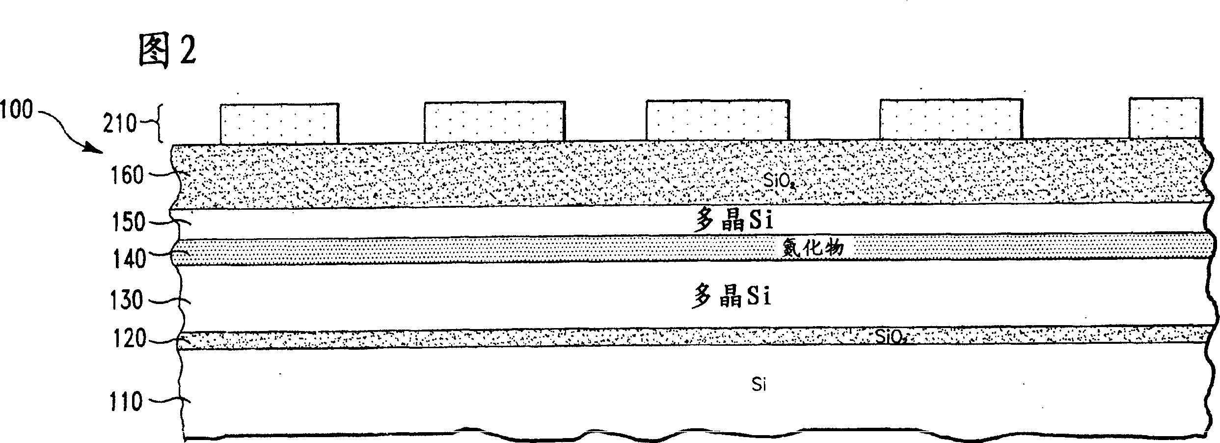
[0009] 1-8C show cross-sectional views of a structure 100 undergoing fabrication steps of a subtractive sidewall image transfer (SIT) process, according to an embodiment of the invention. More particularly, referring to FIG. 1, in one embodiment, as shown, the SIT process begins with a semiconductor substrate 110, a gate dielectric layer 120, a gate electrode layer 130, a hard mask layer 140, a memory layer 150, And the alignment layers 160 are formed one by one thereon. For example, layers 110, 120, 130, 140, 150 and 160 are made of silicon (Si), silicon dioxide (SiO 2 ), polysilicon, silicon nitride, polysilicon, and silicon dioxide.
[0010] Next, referring to FIG. 2 , in one embodiment, a patterned photoresist layer 210 is prepared over the oxide alignment layer 160 by, for example, a photolithographic process.
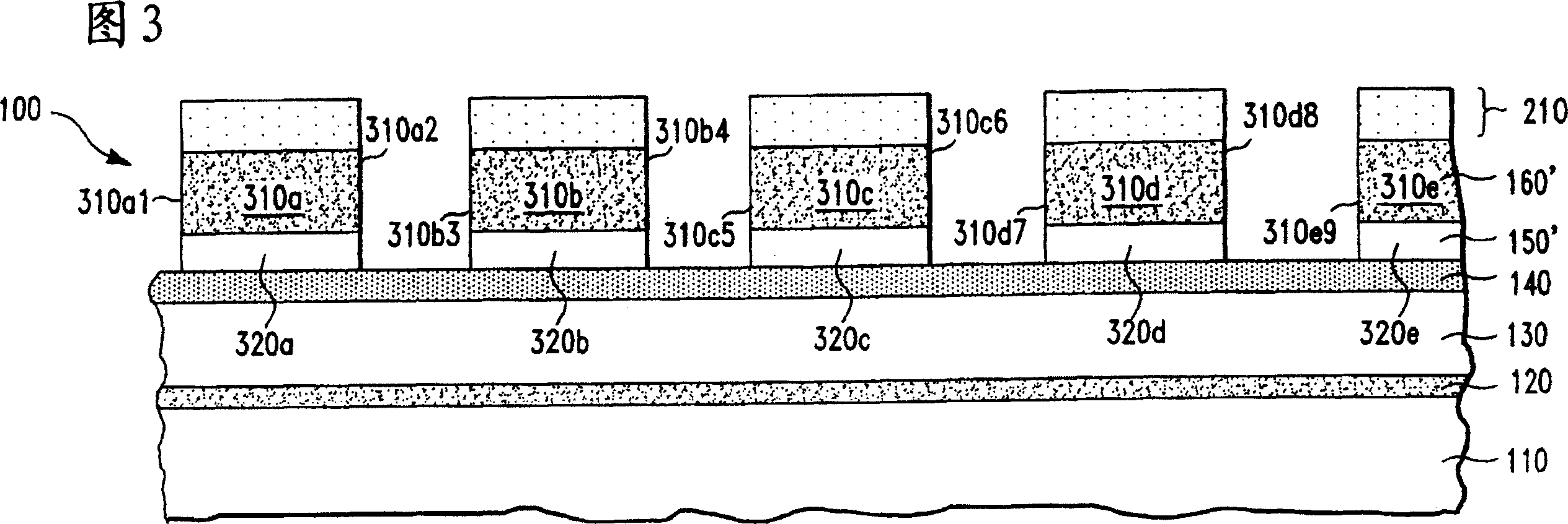
[0011] Next, referring to FIG. 3 , in one embodiment, the oxide positioning layer 160 ( FIG. 2 ) is directionally etched through the patterned photoresist layer...
PUM
 Abstract
Description
Claims
Application Information
 - R&D
- Intellectual Property
- Life Sciences
- Materials
- Tech Scout
- Unparalleled Data Quality
- Higher Quality Content
- 60% Fewer Hallucinations
Browse by: Latest US Patents, China's latest patents, Technical Efficacy Thesaurus, Application Domain, Technology Topic, Popular Technical Reports.
© 2025 PatSnap. All rights reserved.Legal|Privacy policy|Modern Slavery Act Transparency Statement|Sitemap|About US| Contact US: help@patsnap.com