Eureka AIR delivers breakthrough ideas for toughest innovation challenges, trusted by R&D personnel around the world.

Anti-electrostatic method of chip device

An anti-static, chip technology, applied in the direction of static electricity, non-printed electrical components connected to the printed circuit, electrical components, etc., can solve the problem of adding a shielding cover as a whole

Inactive Publication Date: 2007-06-20
ZTE CORP
View PDF0 Cites 0 Cited by
  • Summary
  • Abstract
  • Description
  • Claims
  • Application Information

AI Technical Summary

Problems solved by technology

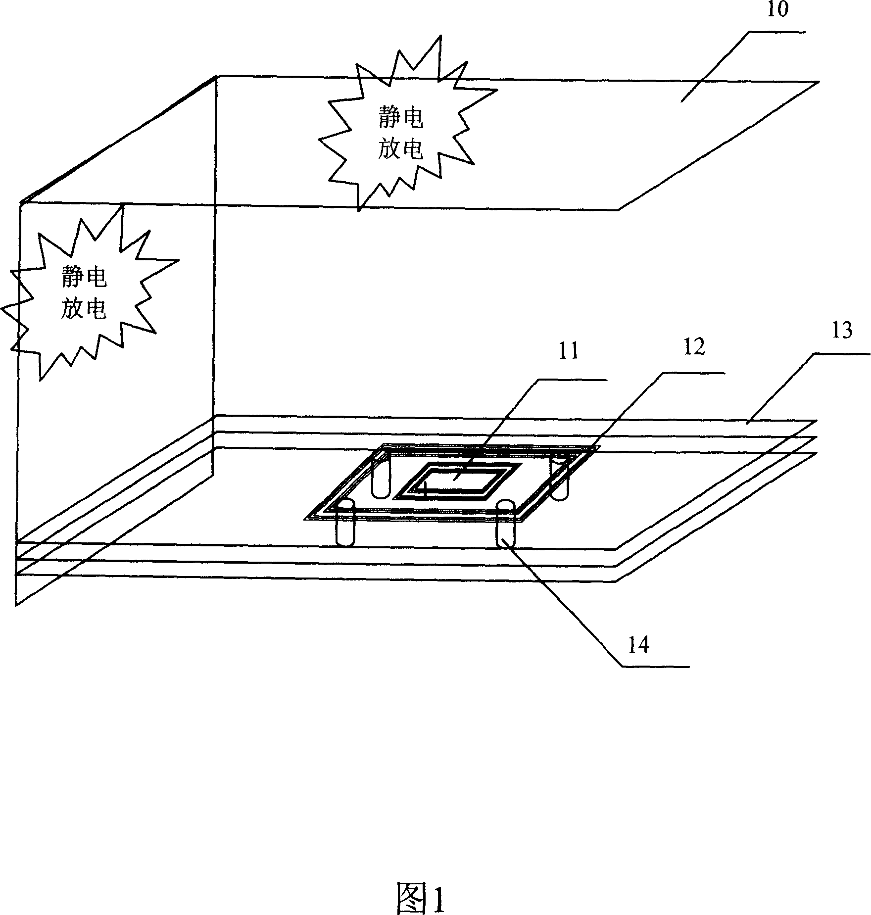
[0003] The technical problem to be solved by the present invention is to provide an anti-static method for chip devices, so as to provide anti-static protection for electronic equipment when it is impossible to add a shield to the whole due to the limitation of the system structure.

Method used


Image

  • Anti-electrostatic method of chip device

Examples


Embodiment Construction

[0019] In order to make the present invention easier to understand, this embodiment is implemented based on the following ideas.

[0020] Static electricity is the static charge on the surface of an object. Static electricity is a kind of electrical energy, which remains on the surface of an object. It is the result of the local imbalance of positive and negative charges, which is formed by the transfer of electrons or ions.

[0021] Electrostatic discharge is the transfer of charge that occurs when objects with different electrostatic potentials approach or pass through direct contact.

[0022] Shielding is made of conductive or magnetically conductive materials such as shells, plates, sleeves, tubes and other shapes to encapsulate the object to be protected, so as to prevent the interference of surrounding electromagnetic energy or prevent unnecessary electromagnetic energy from coupling to other sensitive equipment.

[0023] The protection ground is the loop ground of the...


PUM


Abstract

The first method of the invention is: for a chip connected to circuit board and having a heat-sink, electrically connecting the heat-sink to the ground of the circuit board. The second method of the invention is: mounting a heat-sink on the chip, and then connecting the heat-sink to the ground of the circuit board. The heat-sink is located on the chip and encapsulates the chip, and is connected to the ground through the protected ground or through working ground. When the chip is located in the center of the circuit board, the heat-sink is grounded through working ground; when the chip is located at edge of the circuit board, it is grounded through protected ground.

Description

technical field [0001] The invention relates to an antistatic method, in particular to an antistatic method for a chip device. Background technique [0002] Static electricity is the static charge on the surface of an object. Static electricity is a kind of electrical energy, which remains on the surface of an object. It is the result of the local imbalance of positive and negative charges, which is formed by the transfer of electrons or ions. Electrostatic discharge is the transfer of charge that occurs when objects with different electrostatic potentials approach or pass through direct contact. There are domestic and international mandatory standards for the anti-static capability of communication electronic equipment. The anti-static capability of communication electronic equipment is directly related to whether the communication electronic equipment can be used normally in a complex electromagnetic field environment. Although there are various anti-static methods for ...

Claims


Application Information

Patent Timeline
IPC IPC(8): H05F3/02H05K1/18
Inventor 朱松林
Owner ZTE CORP
Why Eureka
Eureka Blog
Learn More