
Method for cleaning dry film pressed on wafer

A wafer and process technology, applied in the cleaning process field, can solve problems such as inaccurate exposure and affecting exposure quality, and achieve the effect of improving quality

Active Publication Date: 2010-12-08
ADVANCED SEMICON ENG INC
View PDF5 Cites 0 Cited by
  • Summary
  • Abstract
  • Description
  • Claims
  • Application Information

AI Technical Summary

Problems solved by technology

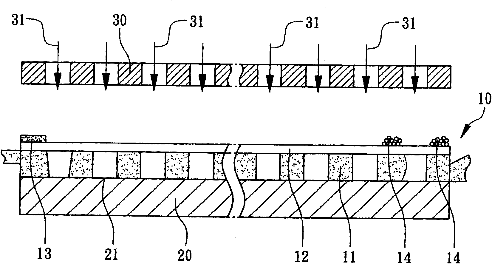
However, before exposure, there will be residual pollutants on the light-transmissive carrier film 12 of the dry film 10, such as residual photoresist 13 and particles 14, and these residual photoresist 13 and particles 14 will cause the exposure radiation 31 to refract or scatter , resulting in inaccurate exposure
In addition, after the conventional dry film 10 is laminated and cut, there will be dry film burrs on its periphery, which will also affect the exposure quality.

Method used


Image

  • Method for cleaning dry film pressed on wafer
  • Method for cleaning dry film pressed on wafer
  • Method for cleaning dry film pressed on wafer

Examples


Embodiment Construction

[0013] The method for using the dry film of the present invention is applicable to the wafer-level packaging process, and a specific embodiment is described below.

[0014] First, see Figure 2A As shown, a dry film 110 is provided, and the dry film 110 mainly includes a structure of at least three layers, which are at least one photoresist layer 111, a light-transmitting carrier film 112, and a protective film 113, wherein the photoresist layer 111 is a A photosensitive resin, which can be a positive photoresist or a negative photoresist, is formed on the light-transmissive carrier film 112 and covered by the protective film 113 . In this embodiment, the photoresist layer 111 is a negative photoresist used as an electroplating bump. Usually, the transparent carrier film 112 can be made of PET (polyester), or can be called Mylar film, and the protective film 113 can be made of PE (polyethylene).

[0015] Afterwards, see Figure 2B As shown, the dry film 110 is laminated to ...


PUM


Abstract

The invention relates to the application of a dry film. It provides a dry film stitching a substrate plate composed of an attached photo resistant layer and an obvious light through carrier mould. Before exposure display, clean the dry film light through carrier mold in the darkroom, with the cleaning method composed of chemical spraying and ion cleansing to get rid of the residue contamination on the photo carrying film, getting rid of the dry film burr to improve the process passing rate of development after subsequent exposure.

Description

【Technical field】 [0001] The present invention relates to a cleaning process of a dry film laminated on a wafer, in particular to a cleaning process of laminating a dry film on a substrate such as a wafer in a wafer-level packaging process. 【Background technique】 [0002] In the field of wafer-level packaging, photoresist materials are usually used for image transfer printing for deposition or etching to form bumps or lines on a wafer. In order to achieve proper thickness and good image effect, the currently used photoresist material is dry film. The traditional dry film has a three-layer structure, which includes a transparent carrier film, at least one photoresist layer and a protective layer, wherein the photoresist layer is interposed between the transparent carrier film and the protective layer. After peeling off the protective layer, the photoresist layer of the dry film is laminated to a substrate (such as a wafer), and then exposed and developed to form a pattern im...

Claims


Application Information

Patent Timeline
Patent Type & Authority Patents(China)
IPC IPC(8): G03F7/00G03F7/26H01L21/56
Inventor 曾琮彦黄敏龙蔡骐隆杨敏智
Owner ADVANCED SEMICON ENG INC
Learn More