Pixel structure
a pixel and structure technology, applied in the field of pixel structure, can solve the problems of low aperture ratio, reduced pixel size, and increased difficulty in wiring design of pixels, and achieve the effect of high aperture ratio
- Summary
- Abstract
- Description
- Claims
- Application Information
AI Technical Summary
Benefits of technology
Problems solved by technology
Method used
Image
Examples
Embodiment Construction
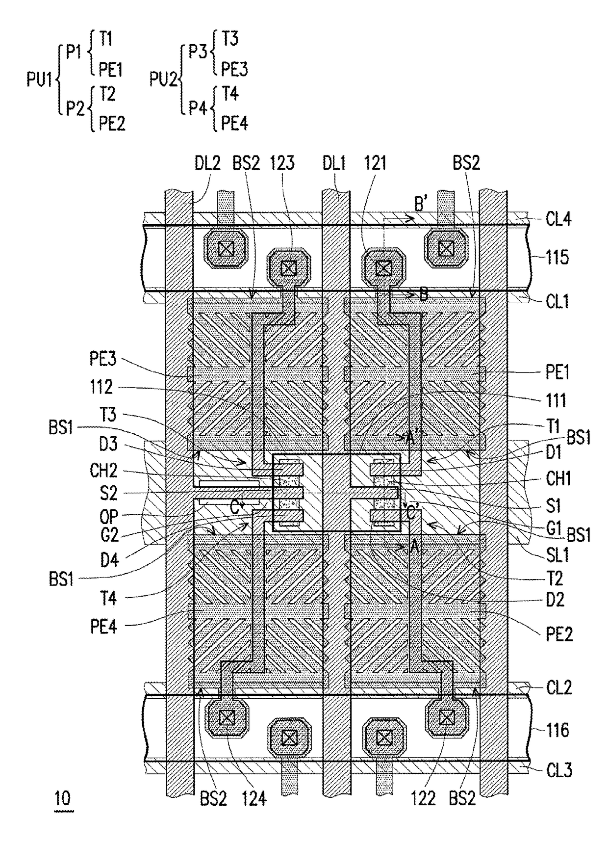
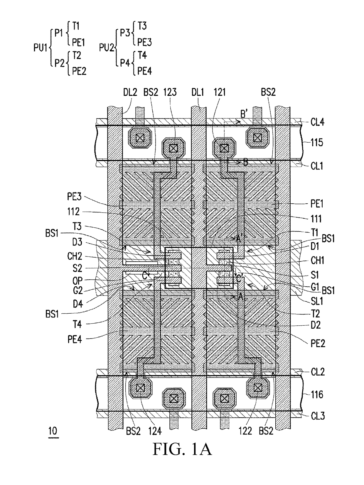
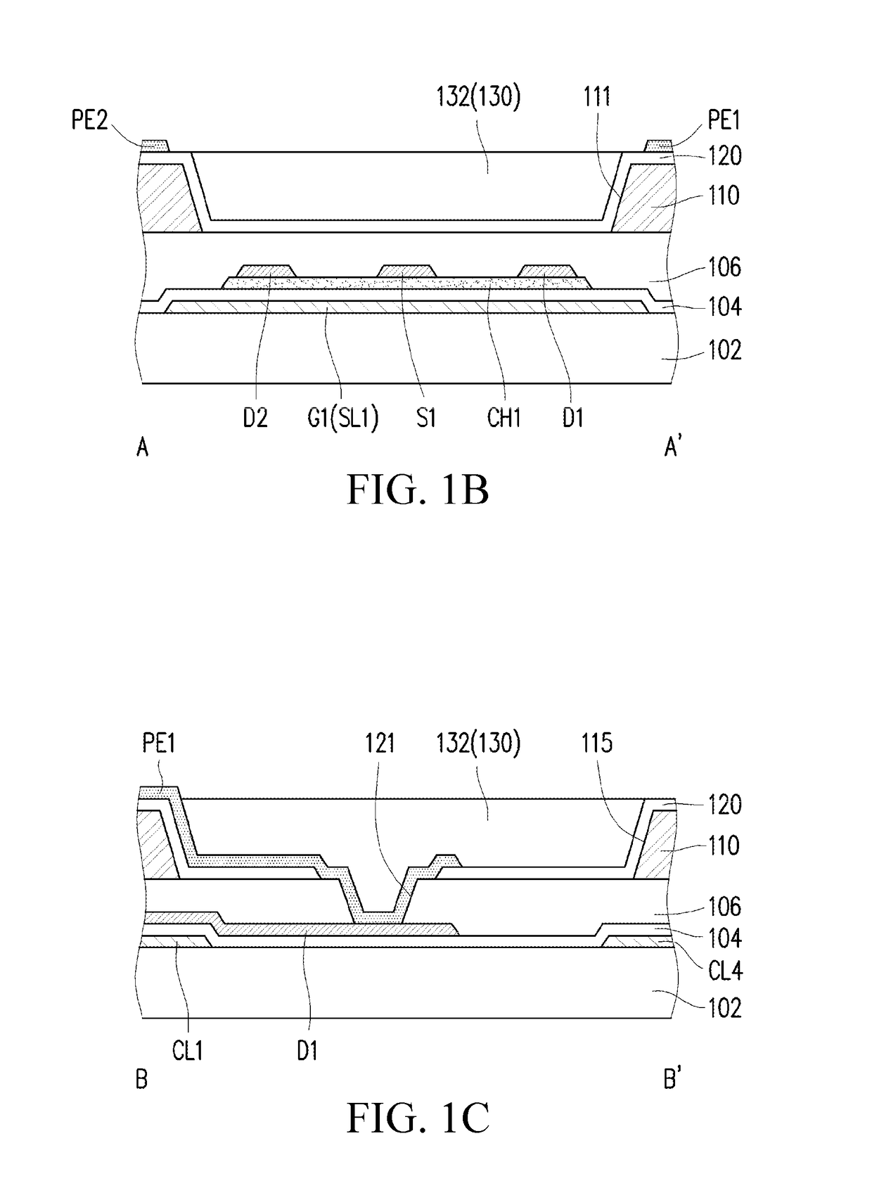
[0041]FIG. 1A is a schematic view of a pixel structure according to an embodiment of the present invention. FIG. 1B to FIG. 1D are respectively schematic cross-sectional views along the lines A-A′, B-B′, and C-C′ in FIG. 1A. With reference to FIG. 1A to FIG. 1D altogether, a pixel structure 10 includes a first scan line SL1, a first data line DL1, a first common line CL1, a second common line CL2, a first pixel unit PU1, a color filter layer 110, and a shielding pattern layer 130 arranged on a substrate 102. The first data line DL1 intersects with the first scan line SL1. The first scan line SL1 is disposed between the first common line CL1 and the second common line CL2.
[0042]The first pixel unit PU1 includes a first sub-pixel P1 and a second sub-pixel P2. The first sub-pixel P1 includes a first active device T1 and a first pixel electrode PE1. The first active device T1 is electrically connected to the first scan line SL1 and the first data line DL1. The first pixel electrode PE1 ...
PUM
 Abstract
Description
Claims
Application Information


