Eureka AIR delivers breakthrough ideas for toughest innovation challenges, trusted by R&D personnel around the world.

Diode

a technology of diodes and diodes, applied in the field of diodes, can solve the problems of voltage ringing and contrarily increasing the number of diodes, and achieve the effect of effectively restraining voltage ringing

Active Publication Date: 2018-09-04
ROHM CO LTD
View PDF8 Cites 2 Cited by
  • Summary
  • Abstract
  • Description
  • Claims
  • Application Information

AI Technical Summary

Benefits of technology

[0005]As an example of measures thereagainst, it is considered that a small number of carriers are implanted from a p layer during a switching operation (recovery operation) by disposing the p layer at a part of an n layer on the cathode side. In other words, carriers are supplied from the p layer during a recovery operation, and, as a result, it is possible to prevent the carriers from being rapidly depleted, and it is possible to restrain a recovery current from being rapidly changed.
[0007]It is an object of the present invention to provide a diode that is capable of effectively restraining voltage ringing during a recovery operation.

Problems solved by technology

As a result, a great change in the electric current occurs, thus causing voltage ringing.
However, there is a possibility that voltage ringing will contrarily become large merely by disposing the p layer, and therefore it is necessary to pay attention to the size or the disposition rate of the p layer with respect to the disposition of the p layer.

Method used


Image

  • Diode
  • Diode
  • Diode

Examples


Embodiment Construction

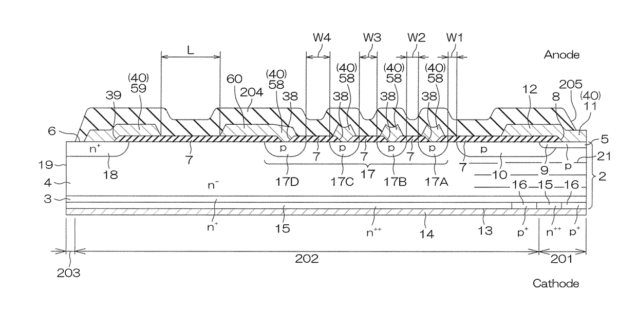
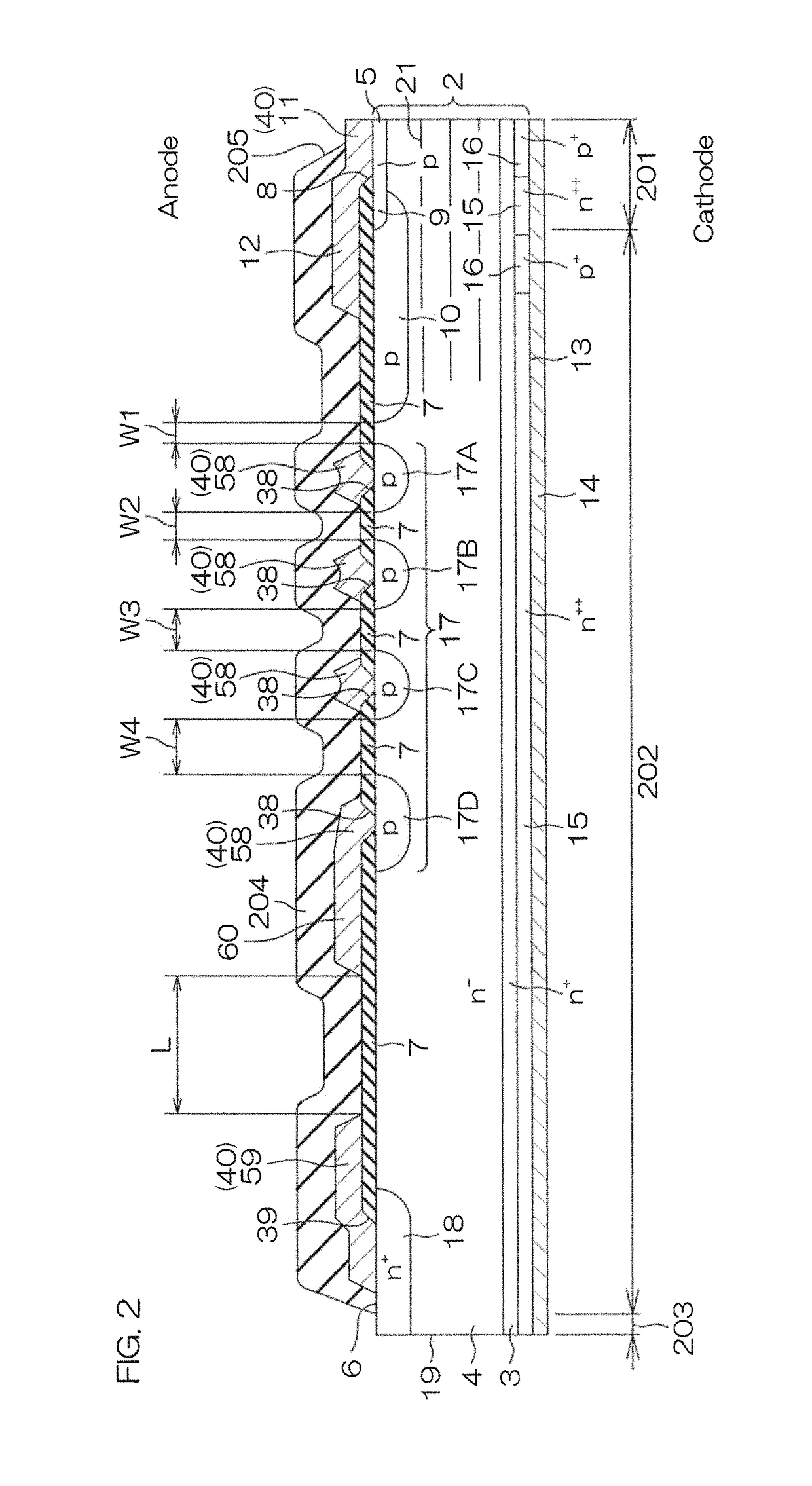
[0032]A diode according to a preferred embodiment of the present invention includes an n type semiconductor layer including an n type cathode layer and an n type drift layer that is disposed on the n type cathode layer and that has an impurity concentration lower than the n type cathode layer, a p type anode layer disposed at a surface part of the n type drift layer, a p type hole implantation layer selectively disposed at the n type cathode layer, an anode electrode electrically connected to the p type anode layer, and a cathode electrode electrically connected to the n type cathode layer and to the p type hole implantation layer, and the p type hole implantation layer has a diameter of 20 μm or more.

[0033]For example, an electron implanted from the n type cathode layer into the n type drift layer when an electric current is conducted in the forward direction moves to the n type cathode layer along the thickness direction of the n type drift layer during a switching operation. At t...


PUM


Abstract

A diode includes an n type semiconductor layer including an n type cathode layer and an n type drift layer that has an impurity concentration lower than the n type cathode layer and that is disposed on the n type cathode layer, a p type anode layer disposed at a surface part of the n type drift layer, a p type hole implantation layer selectively disposed at the n type cathode layer, an anode electrode electrically connected to the p type anode layer, and a cathode electrode electrically connected to the n type cathode layer and to the p type hole implantation layer, and the p type hole implantation layer has a diameter of 20 μm or more.

Description

CROSS-REFERENCE TO RELATED APPLICATIONS[0001]The present application corresponds to Japanese Patent Application No. 2016-64021 filed in the Japan Patent Office on Mar. 28, 2016, and the entire disclosure of the application is incorporated herein by reference.TECHNICAL FIELD[0002]The present invention relates to a diode, and in particular to a diode having a short reverse recovery time trr that is called a fast recovery diode (FRD).BACKGROUND ART[0003]A fast recovery diode is publicly known, and is used for the rectification of a high-frequency power source or the like. Among conventional fast recovery diodes, there are diodes that have realized excellent on-off characteristics by introducing a life time killer by means of electron irradiation in order to shorten a reverse recovery time trr during a switching operation (for example, Japanese Patent Application Publication No. 2005-183605).SUMMARY OF INVENTION[0004]In a diode, electrons implanted from a cathode into a drift layer duri...

Claims


Application Information

Patent Timeline
Patent Type & Authority Patents(United States)
IPC IPC(8): H01L29/66H01L29/87H01L29/06H01L29/40H01L29/861H01L29/16H01L29/36
CPCH01L29/87H01L29/0615H01L29/0619H01L29/0623H01L29/0688H01L29/1608H01L29/404H01L29/8611H01L29/0692H01L29/36H01L29/0638
Inventor UMEKI, SHINYA
Owner ROHM CO LTD
Why Eureka
Eureka Blog
Learn More