Eureka AIR delivers breakthrough ideas for toughest innovation challenges, trusted by R&D personnel around the world.

Diode

Active Publication Date: 2017-09-28
ROHM CO LTD
View PDF4 Cites 2 Cited by
  • Summary
  • Abstract
  • Description
  • Claims
  • Application Information

AI Technical Summary

Benefits of technology

The patent text describes a method for reducing voltage ringing during a recovery operation in a diode. The method involves implanting a small number of carriers from a specific layer during the recovery operation. This helps to prevent the carriers from being rapidly depleted and reduces the change in recovery current. The technical effect is a more effective restraint on voltage ringing during recovery.

Problems solved by technology

As a result, a great change in the electric current occurs, thus causing voltage ringing.
However, there is a possibility that voltage ringing will contrarily become large merely by disposing the p layer, and therefore it is necessary to pay attention to the size or the disposition rate of the p layer with respect to the disposition of the p layer.

Method used


Image

  • Diode
  • Diode
  • Diode

Examples


Embodiment Construction

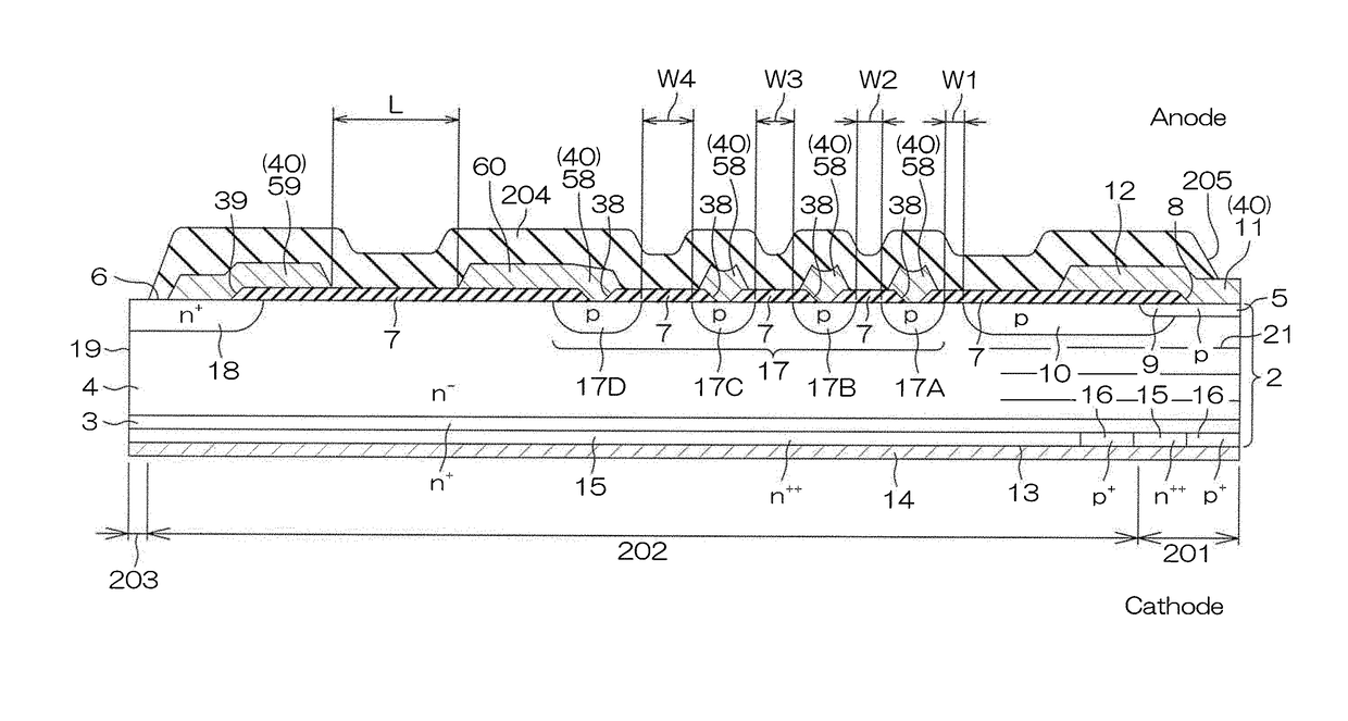
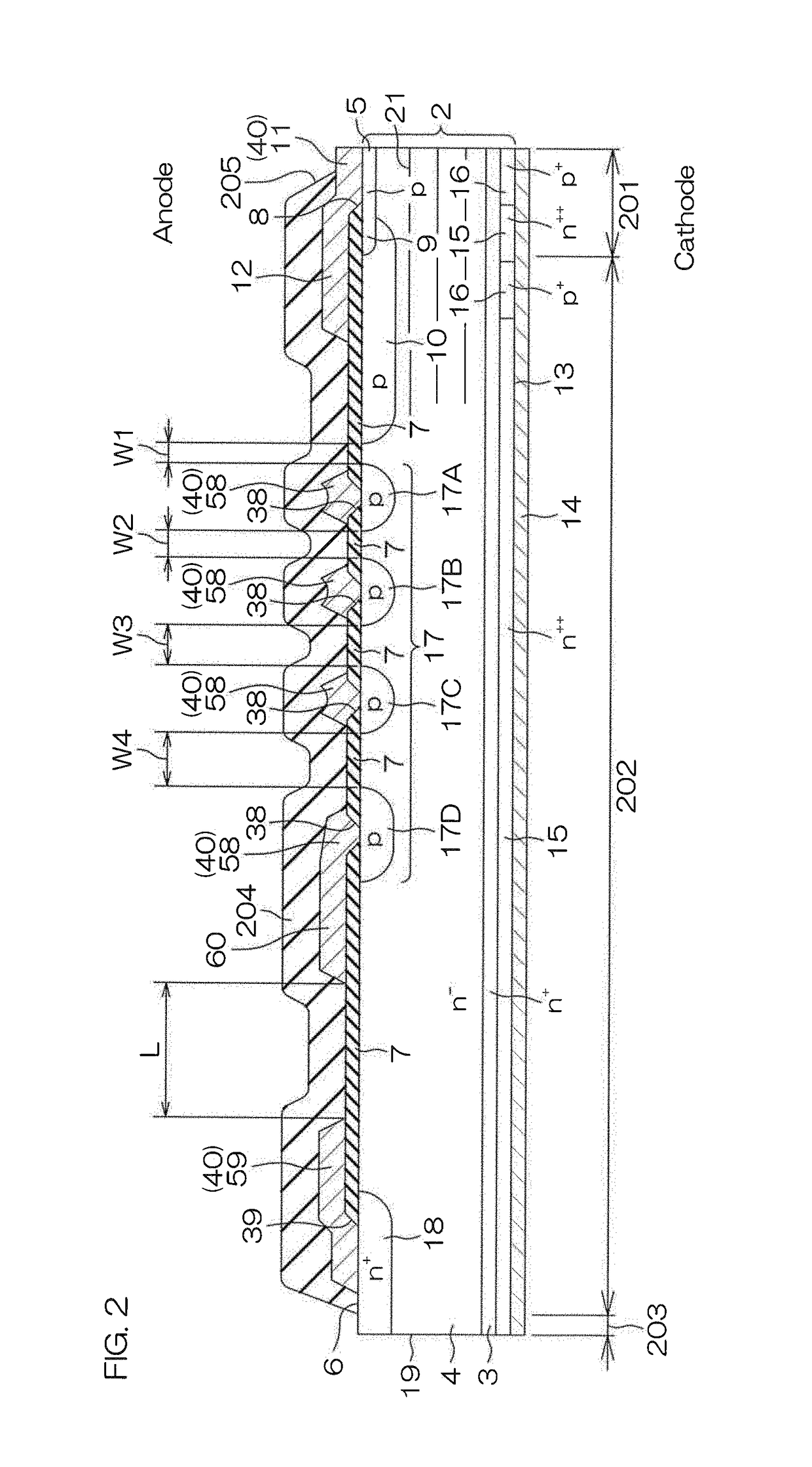
[0032]A diode according to a preferred embodiment of the present invention includes an n type semiconductor layer including an n type cathode layer and an n type drift layer that is disposed on the n type cathode layer and that has an impurity concentration lower than the n type cathode layer, a p type anode layer disposed at a surface part of the n type drift layer, a p type hole implantation layer selectively disposed at the n type cathode layer, an anode electrode electrically connected to the p type anode layer, and a cathode electrode electrically connected to the n type cathode layer and to the p type hole implantation layer, and the p type hole implantation layer has a diameter of 20 μm or more.

[0033]For example, an electron implanted from the n type cathode layer into the n type drift layer when an electric current is conducted in the forward direction moves to the n type cathode layer along the thickness direction of the n type drift layer during a switching operation. At t...


PUM


Abstract

A diode includes an n type semiconductor layer including an n type cathode layer and an n type drift layer that has an impurity concentration lower than the n type cathode layer and that is disposed on the n type cathode layer, a p type anode layer disposed at a surface part of the n type drift layer, a p type hole implantation layer selectively disposed at the n type cathode layer, an anode electrode electrically connected to the p type anode layer, and a cathode electrode electrically connected to the n type cathode layer and to the p type hole implantation layer, and the p type hole implantation layer has a diameter of 20 μm or more.

Description

CROSS-REFERENCE TO RELATED APPLICATIONS[0001]The present application corresponds to Japanese Patent Application No. 2016-64021 filed in the Japan Patent Office on Mar. 28, 2016, and the entire disclosure of the application is incorporated herein by reference.TECHNICAL FIELD[0002]The present invention relates to a diode, and in particular to a diode having a short reverse recovery time trr that is called a fast recovery diode (FRD).BACKGROUND ART[0003]A fast recovery diode is publicly known, and is used for the rectification of a high-frequency power source or the like. Among conventional fast recovery diodes, there are diodes that have realized excellent on-off characteristics by introducing a life time killer by means of electron irradiation in order to shorten a reverse recovery time trr during a switching operation (for example, Japanese Patent Application Publication No. 2005-183605).SUMMARY OF INVENTION[0004]In a diode, electrons implanted from a cathode into a drift layer duri...

Claims


Application Information

Patent Timeline
IPC IPC(8): H01L29/87H01L29/06
CPCH01L29/87H01L29/0692H01L29/0688H01L29/0623H01L29/36H01L29/404H01L29/8611H01L29/0615H01L29/0619H01L29/0638H01L29/1608
Inventor UMEKI, SHINYA
Owner ROHM CO LTD
Why Eureka
Eureka Blog
Learn More