Array substrate, manufacturing method thereof, and display device

a technology of array substrate and manufacturing method, applied in the field of array substrate, can solve the problems of low transmittance and display delay

Active Publication Date: 2018-12-11
BOE TECH GRP CO LTD +1
View PDF24 Cites 0 Cited by
  • Summary
  • Abstract
  • Description
  • Claims
  • Application Information

AI Technical Summary

Benefits of technology

The invention provides an array substrate, a method to make it, and a display device that overcomes the challenges of low transmittance and display delay caused by difficulty in driving liquid crystals between pixel electrodes on a conventional array substrate.

Problems solved by technology

As a gate line or a data line is provided between two adjacent sub-pixel areas, the electric field at the positions corresponding to the gate line and the data line is weak, and therefore, it is difficult to drive the liquid crystals, resulting in problems such as low transmittance, display delay and the like.

Method used


Image

  • Array substrate, manufacturing method thereof, and display device
  • Array substrate, manufacturing method thereof, and display device
  • Array substrate, manufacturing method thereof, and display device

Examples


Embodiment Construction

[0024]The technical solutions in the embodiments of the present invention will be described clearly and completely below in conjunction with the accompanying drawings in the embodiments of the present invention, and obviously, the described embodiments are merely a part, not all of the embodiments of the present invention. Based on the embodiments in the present invention, all other embodiments obtained by those skilled in the art without creative efforts are within the protection scope of the present invention.

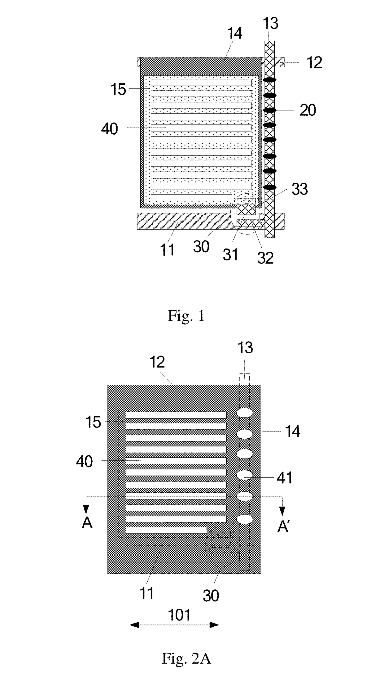
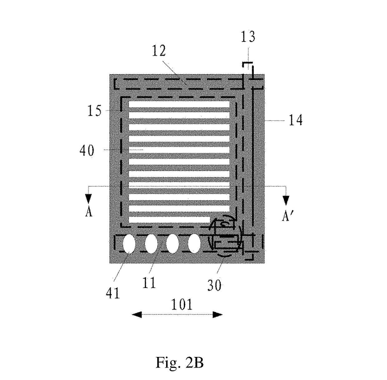
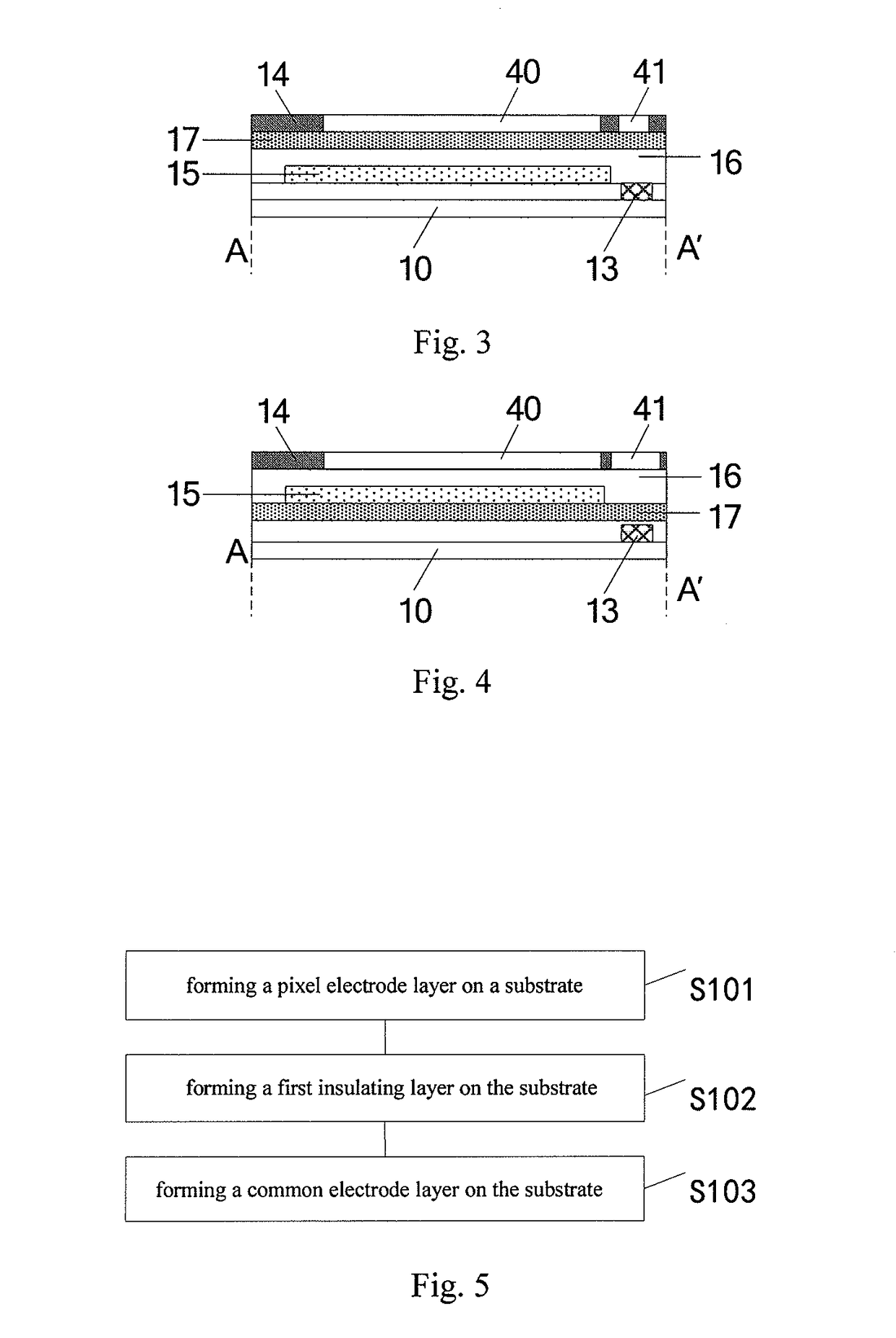
[0025]FIG. 2 is a top view of one sub-pixel area of an array substrate according to an embodiment of the present invention; FIG. 3 is a sectional view of one sub-pixel area of an array substrate according to an embodiment of the present invention. As shown in FIGS. 2 and 3, an array substrate according to an embodiment of the present invention comprises a glass substrate 10 and gate lines 11, common electrode lines 12, pixel electrodes 15 and a common electrode 14 formed ther...


PUM

PropertyMeasurementUnit
uniformityaaaaaaaaaa

Abstract

The present invention provides an array substrate, a manufacturing method thereof and a display device, relates to the field of display technology. The array substrate comprises: a substrate; a gate metal layer comprising gate lines; a source and drain metal layer comprising data lines, the gate lines and the data lines intersecting with each other to define a plurality of sub-pixel areas; a pixel electrode layer provided on the substrate, which comprises a plurality of pixel electrodes which are in one-to-one correspondence with the plurality of sub-pixel areas; a common electrode layer provided on the substrate, which is provided with a plurality of cutting hole at positions corresponding to spaces between the pixel electrodes; a first insulating layer provided between the pixel electrode layer and the common electrode layer; and a second insulating layer provided between the gate metal layer and the source and drain metal layer.

Description

FIELD OF THE INVENTION[0001]The present invention relates to the field of display technology, and particularly to an array substrate, a manufacturing method thereof and a display device.BACKGROUND OF THE INVENTION[0002]Compared to common liquid crystal display techniques, ADS (Advanced-super Dimensional Switching) display technique can provide wider angle of view, higher transmittance, shorter response time and higher brightness and contrast, and is therefore becoming more popular.[0003]In an ADS-LCD (Advanced-Super Dimensional Switching-Liquid Crystal Display), pixel electrodes and common electrodes are formed in an array substrate, and may generate a multi-dimensional electric filed for driving liquid crystals, thus achieving a display function.[0004]FIG. 1 illustrates a structure of one sub-pixel area of an array substrate of an ADS-LCD, and the structure comprises a gate line 11, a common electrode line 12, a data line 13, a thin film transistor 30 (the region in the dashed circ...

Claims


Application Information

Patent Timeline
Patent Type & Authority Patents(United States)
IPC IPC(8): H01L31/20H01L29/66H01L29/80H01L27/146H01L31/036G02F1/1343G02F1/1362H01L27/12H01L29/786
CPCH01L27/124G02F1/1362G02F1/134309H01L29/786H01L27/1259H01L29/66742H01L27/1248
Inventor WANG, ZHENG
Owner BOE TECH GRP CO LTD
Why Eureka
Try Eureka