Inorganic LED pixel structure

a pixel structure and led pixel technology, applied in the field of pixel structure and display, can solve the problems of reducing the optical sharpness of the display, and even 50% of the photons formed in the diode junction can be trapped and ultimately lost in such structures, so as to improve the image quality and contrast, reduce manufacturing costs, and improve emission efficiency

Active Publication Date: 2019-01-29
X DISPLAY CO TECH LTD
View PDF361 Cites 4 Cited by
  • Summary
  • Abstract
  • Description
  • Claims
  • Application Information

AI Technical Summary

Benefits of technology

[0020]The present invention provides improved image quality and contrast, emission efficiency, and a reduced manufacturing cost in a mechanically and environmentally robust structure useful in a display system.

Problems solved by technology

More than 40% or even 50% of the photons formed in a diode junction can be trapped and ultimately lost in such structures.
Furthermore, light emitted by one pixel can propagate through a substrate and be emitted near another pixel, reducing the optical sharpness of the display.
Such multi-layer structures are more complex and costly to manufacture and the additional layers can also absorb emitted light, reducing display efficiency.

Method used


Image

  • Inorganic LED pixel structure
  • Inorganic LED pixel structure
  • Inorganic LED pixel structure

Examples


Embodiment Construction

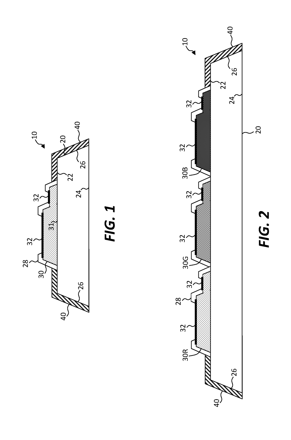
[0083]Referring to the cross section of FIG. 1, in an embodiment of the present invention an inorganic light-emitting diode (iLED) pixel structure 10 includes a transparent pixel substrate 20 having an LED surface 22, an emission surface 24 opposite the LED surface 22, and one or more sides 26 other than the LED surface 22 and the emission surface 24 that are not parallel to the LED surface 22 or the emission surface 24. The sides 26, the LED surface 22, or emission surface 24 can be facets of a three-dimensional solid.

[0084]An inorganic light-emitting diode (iLED) 30 is mounted or disposed on the pixel substrate 20. The iLED 30 has an emission side 31 adjacent to or in contact with the LED surface 22 of the pixel substrate 20. The iLED 30 emit lights into the pixel substrate 20 through the emission side 31 of the iLED 30. The emitted light passes into the pixel substrate 20 through the LED surface 22 of the pixel substrate 20 and out of the pixel substrate 20 through the emission s...


PUM


Abstract

An inorganic light-emitting diode (iLED) pixel structure includes a transparent pixel substrate having an LED surface, an emission surface opposite the LED surface, and one or more sides other than the LED surface and the emission surface that are not parallel to the LED surface or the emission surface. One or more iLEDs are mounted on the pixel substrate and each iLED has an emission side adjacent to the LED surface of the pixel substrate to emit light into the pixel substrate and out of the emission surface. A reflector is disposed on at least a portion of the one or more sides.

Description

PRIORITY APPLICATION[0001]This application claims priority to and benefit of U.S. Patent Application No. 62 / 301,077, filed Feb. 29, 2016, entitled Inorganic LED Pixel Structure, the content of which is incorporated herein by reference in its entirety.CROSS REFERENCE TO RELATED APPLICATION[0002]Reference is made to U.S. patent application Ser. No. 14 / 818,201, entitled Inorganic-Light-Emitter Display with Integrated Black Matrix by Bower et al., the content of which is incorporated herein by reference in its entirety.FIELD OF THE INVENTION[0003]The present invention relates to a pixel structure and display including inorganic light emitters with improved light emission.BACKGROUND OF THE INVENTION[0004]Flat-panel displays are widely used in conjunction with computing devices, in portable devices, and for entertainment devices such as televisions. Such displays typically employ a plurality of pixels distributed over a display substrate to display images, graphics, or text. For example, ...

Claims


Application Information

Patent Timeline
Patent Type & Authority Patents(United States)
IPC IPC(8): H01L29/20H01L33/00H01L33/46H01L25/075
CPCH01L33/46H01L25/0753H01L2224/81
Inventor BOWER, CHRISTOPHERCOK, RONALD S.
Owner X DISPLAY CO TECH LTD
Why Eureka
Try Eureka