Supercharge Your Innovation With Domain-Expert AI Agents!

Electro-optic display backplane structure with drive components and pixel electrodes on opposed surfaces

a backplane structure and drive component technology, applied in the field of electro-optic display, can solve the problems of inadequate service life of these displays, preventing widespread use, and gas-based electrophoretic media appearing to be susceptible to the same types of problems

Active Publication Date: 2019-06-11
E INK CORPORATION
View PDF240 Cites 1 Cited by
  • Summary
  • Abstract
  • Description
  • Claims
  • Application Information

AI Technical Summary

Problems solved by technology

Nevertheless, problems with the long-term image quality of these displays have prevented their widespread usage.
For example, particles that make up electrophoretic displays tend to settle, resulting in inadequate service-life for these displays.
Such gas-based electrophoretic media appear to be susceptible to the same types of problems due to particle settling as liquid-based electrophoretic media, when the media are used in an orientation which permits such settling, for example in a sign where the medium is disposed in a vertical plane.
Indeed, particle settling appears to be a more serious problem in gas-based electrophoretic media than in liquid-based ones, since the lower viscosity of gaseous suspending fluids as compared with liquid ones allows more rapid settling of the electrophoretic particles.
However, the methods used for assembling LCD's cannot be used with encapsulated electrophoretic displays.
This LCD assembly process cannot readily be transferred to encapsulated displays.
Electro-optic displays, including electrophoretic displays, can be costly; for example, the cost of the color LCD found in a portable computer is typically a substantial fraction of the entire cost of the computer.
Such large area displays are frequently formed by “tiling” (i.e., juxtaposing) a two-dimensional array of discrete electro-optic displays together since, for technical reasons, such as limitations on the size of backplanes produced by photolithography, individual electro-optic displays cannot economically exceed a certain size.
Unfortunately, conventional electro-optic displays require driver electronics which are normally disposed around the periphery of the display.
However, such peripheral driver electronics do create a problem when multiple displays are used to form a large area display since the peripheral areas are inherently optically inactive.
However, manufacturing cost associated with either methods may prevent them being used for backplanes where pixel or pixel segment designs are unique (e.g., large sized display signs) and only a few such backplane are needed.
For example, the tooling cost associated with screen printing may amount to hundreds or thousands of dollars, making it prohibitively expensive for manufacturing backplane designs where only a few backplanes are needed for specific applications.
Furthermore, both screen printing or PCB manufacturing are limited to assemble backplanes of 24 inches by 48 inches or less in size for majority of manufacturers.
In some instances, larger sized PCBs can be assembled but again the manufacturing cost may be prohibitively expensive if only a few units are needed.

Method used


Image

  • Electro-optic display backplane structure with drive components and pixel electrodes on opposed surfaces
  • Electro-optic display backplane structure with drive components and pixel electrodes on opposed surfaces
  • Electro-optic display backplane structure with drive components and pixel electrodes on opposed surfaces

Examples


Embodiment Construction

[0049]The use of electro-optic display technology is expanding beyond electronic document reader applications to a variety of electronic display products including product labels, retail shelf labels, device monitoring indicators, wristwatches, signs, and promotional or advertising displays. Typically, electro-optic displays are encased by a frame or a bezel to hide the electrical connections of the display which generally lay alongside the display. In some applications, specifically, large scale tiled displays, it is generally preferred that the entire viewing area of an electro-optic display be optically active; for example, a billboard made by tiling a plurality of electro-optic displays together to create a large display, where the entire viewing surface of each individual display is optically active and the space between each display is minimized, such that the large display appears as a single continuous display.

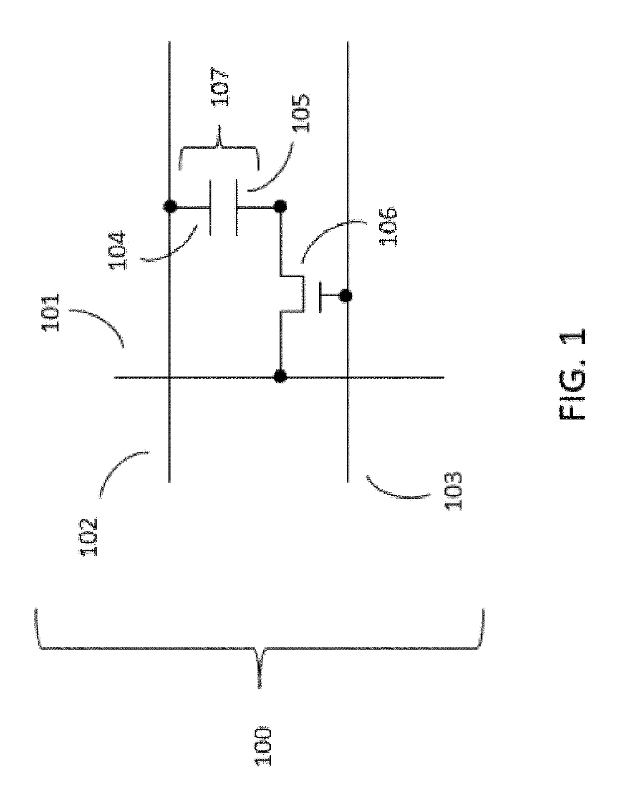
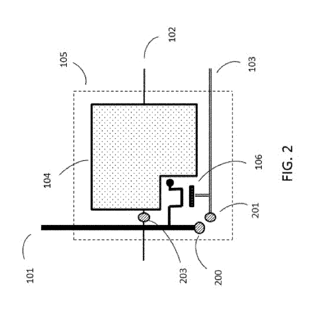
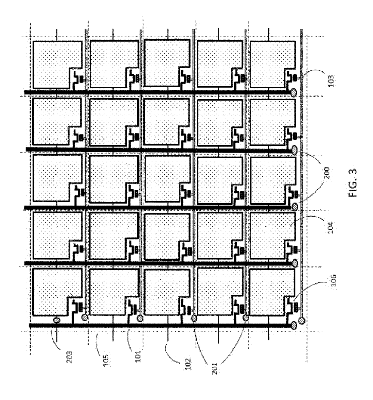
[0050]Accordingly, this invention provides for an electro-optic d...


PUM

PropertyMeasurementUnit
sizeaaaaaaaaaa
sizeaaaaaaaaaa
sizeaaaaaaaaaa

Abstract

The subject matter presented herein relates to a method for producing a backplane for electro-optic displays. The method may include providing a substrate coated with a first conductive material on a first side and a second conductive material on a second side, the second side being positioned opposite from the first side, patterning the first conductive material by cutting through the first conductive material, wherein the patterning of the first conductive material creates electrical isolated conductive segments to be controlled by a driver circuit and creating a plurality of vias on the substrate, the plurality of vias extending through the substrate and providing electrical conductivity between the first and second sides. The method may further include creating a plurality of conductive traces on the second side of the substrate by patterning the second conductive material by locally align the vias to the driver circuit.

Description

REFERENCE TO RELATED APPLICATIONS[0001]This application claims priority to U.S. Provisional Application 62 / 319,685 filed on Apr. 7, 2016. This application is also a continuation in part application to U.S. patent application Ser. No. 14 / 615,617 filed on Feb. 6, 2015. The Ser. No. 14 / 615,617 application itself claims priority to U.S. Patent Application No. 61 / 937,168, filed Feb. 7, 2014. The entire contents of this applications mentioned herein, and of all other U.S. patents and published and copending applications mentioned below, are herein incorporated by reference.BACKGROUND OF INVENTION[0002]In applications where individual electro-optic displays are filed together to create a larger display, it is optimal for the viewing area to be completely active. Accordingly, this invention relates to an electro-optic display having a backplane with circuit elements on at least two surfaces, a plurality of pixels arranged in a matrix on the front surface of the backplane, at least one drive...

Claims


Application Information

Patent Timeline
Patent Type & Authority Patents(United States)
IPC IPC(8): H05K3/40G02F1/1345G02F1/167H05K3/02G02F1/1362H05K3/12
CPCG02F1/167G02F1/13452G02F1/136286H05K3/027H05K2203/166H05K3/12H05K3/4053H05K2201/09363H05K2203/107G02F2001/136295G02F1/13336G02F1/1676G02F1/136295
Inventor PAOLINI, JR., RICHARD J.HARRIS, GEORGE G.JACOBSEN, KEITH A.GALE, HENRY WARE
Owner E INK CORPORATION
Features
  • R&D
  • Intellectual Property
  • Life Sciences
  • Materials
  • Tech Scout
  • Unparalleled Data Quality
  • Higher Quality Content
  • 60% Fewer Hallucinations
Learn More