Check patentability & draft patents in minutes with Patsnap Eureka AI!

Method and apparatus for simulation of lithography overlay

a technology of overlay and simulation method, applied in the direction of photomechanical exposure apparatus, material analysis, instruments, etc., can solve the problems of non-uniform stress being applied to semiconductor wafers, shrinking of overlay budgets, and increasing manufacturing processes, so as to achieve the effect of optimizing the throughput of the lithography process

Active Publication Date: 2019-08-13
QONIAC
View PDF32 Cites 0 Cited by
  • Summary
  • Abstract
  • Description
  • Claims
  • Application Information

AI Technical Summary

Benefits of technology

[0013]The teachings of the disclosure provide a method for simulation of lithography overlay that enables simulations of alternative overlay measurements to be carried out. This in turn allows the testing of assumptions regarding the number of measurement that need to be carried out as well as potentially providing a control method for optimising the throughput of the lithography process.

Problems solved by technology

Current trends in the processing of the semiconductor wafers means that overlay budgets shrink with shrinking ground rules, and manufacturing processes are becoming more aggressive.
The non-uniformity of some manufacturing processes over the semiconductor wafer surface and a plurality of manufacturing process steps may result in non-uniform stress being applied to the semiconductor wafer.
However, complete overlay measurements are very slow to perform, so they may cause a tool capacity problem.
However, there will be a resultant reduction in the accuracy of the measurements and thus a reduction in the reliability of any values calculated from an interpolation of the measurements.
This assumption is not always valid.

Method used


Image

  • Method and apparatus for simulation of lithography overlay
  • Method and apparatus for simulation of lithography overlay
  • Method and apparatus for simulation of lithography overlay

Examples


Embodiment Construction

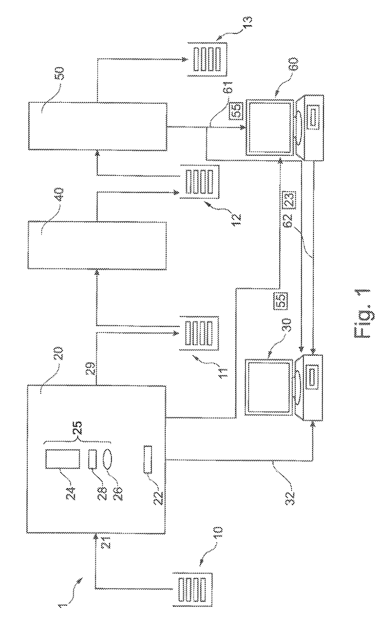
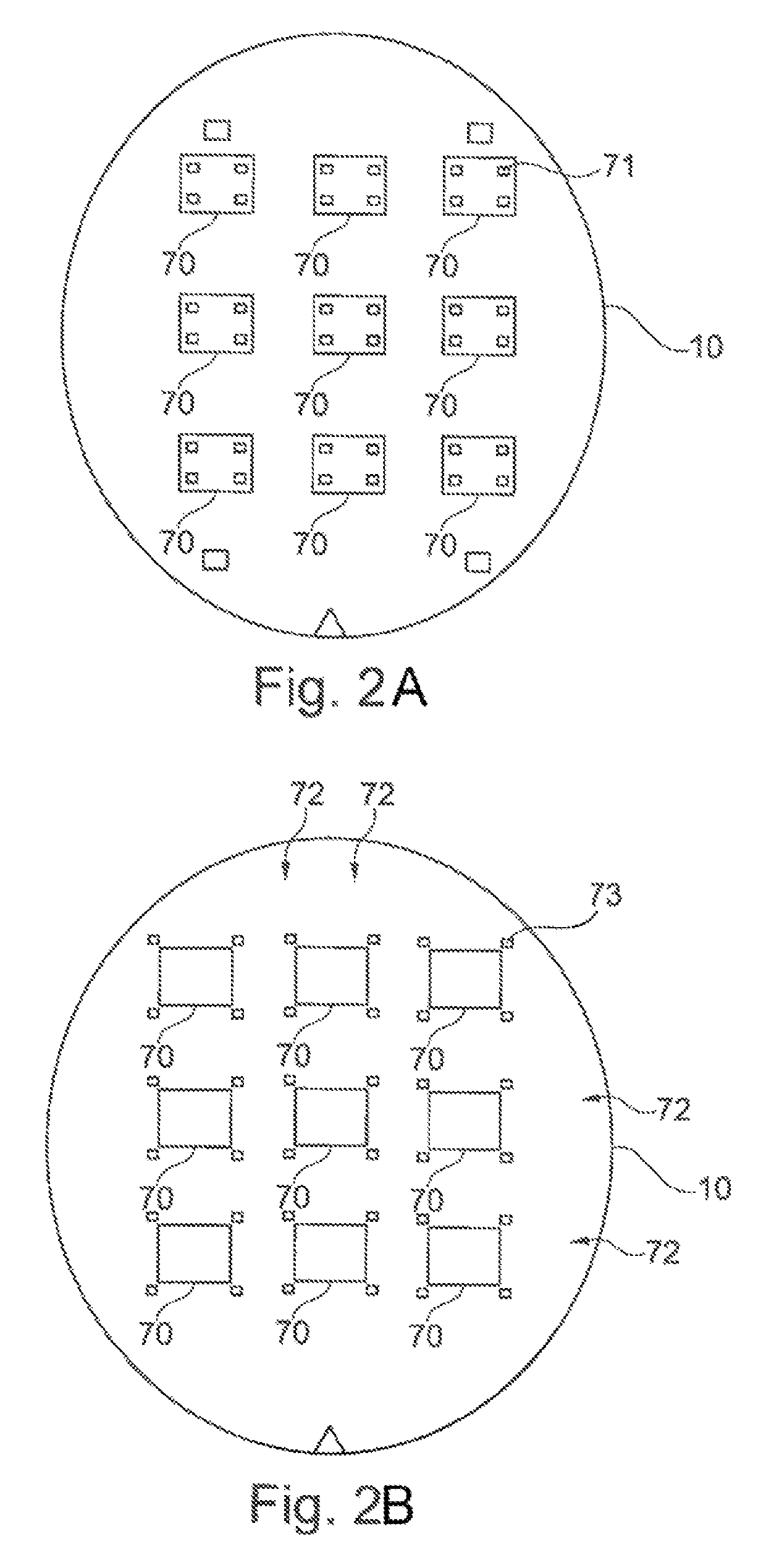
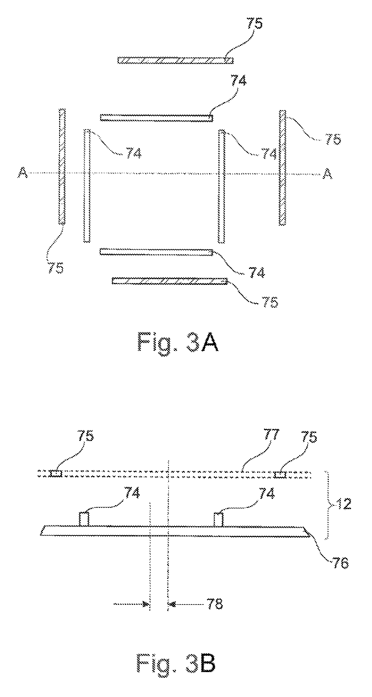
[0026]The invention will now be described on the basis of the drawings. It will be understood that the embodiments and aspects of the invention described herein are only examples and do not limit the protective scope of the claims in any way. The invention is defined by the claims and their equivalents. It will be understood that features of one aspect or embodiment of the invention can be combined with a feature of a different aspect or aspects and / or embodiments of the invention.

[0027]In the following, embodiments and / or implementations of the method and the apparatus are described with respect to simulating overlay measurements during a lithography step whilst manufacturing a semiconductor device on a semiconductor wafer. The embodiments, however, might also be useful in other respects, e.g., improvements in process control, improvements in identifying lot to lot variations of a layout pattern, yield enhancement techniques or the like.

[0028]Furthermore, it should be noted that th...


PUM

PropertyMeasurementUnit
aspect ratioaaaaaaaaaa
stressaaaaaaaaaa
semiconductoraaaaaaaaaa

Abstract

A method for simulation of lithography overlay is disclosed which comprises storing alignment parameters used to align a semiconductor wafer prior to a lithography step; storing process control parameters used during the lithography step on the semiconductor wafer; storing overlay parameters measured after the lithography step; calculating alternative alignment parameters and alternative process control parameters. The alternative alignment parameters and the alternative process control parameters are added to cleansed overlay parameters to obtain simulated lithography overlay data.

Description

CROSS-REFERENCE TO RELATED APPLICATIONS[0001]The present application claims the benefit of the filing date of U.S. Provisional Patent Application Ser. No. 61 / 669,372 filed by the present inventor on Jul. 9, 2012.[0002]The aforementioned provisional patent application is hereby incorporated by reference in its entirety.[0003]This patent application additionally is related to U.S. Non-Provisional application Ser. No. 13 / 749,740 entitled “Method and Apparatus for Fabricating Wafers” and filed on 25 Jan. 2013, Now U.S. Pat. No. 9,543,223, which hereby is incorporated by reference herein.FIELD OF THE INVENTION[0004]This field of the present application relates in general to a method for the simulation of a lithography overlay and an apparatus for the simulation of a lithography overlay on the surface of a semiconductor wafer.BACKGROUND OF THE INVENTION[0005]It will be appreciated that the term “semiconductor wafer” as used in this disclosure is intended to imply wafers used in the manufa...

Claims


Application Information

Patent Timeline
Patent Type & Authority Patents(United States)
IPC IPC(8): G03F9/00G01N21/95G03F7/20
CPCG03F7/70633G01N21/9501G03F9/7003G03F9/7046G03F7/705G03F9/7088
Inventor HABETS, BORIS
Owner QONIAC
Features
  • R&D
  • Intellectual Property
  • Life Sciences
  • Materials
  • Tech Scout
  • Unparalleled Data Quality
  • Higher Quality Content
  • 60% Fewer Hallucinations
Learn More