Surface wave launcher comprising a waveguide with a planar conducting layer having one or more slots disposed therein

a launcher and planar conducting technology, applied in waveguide devices, leaky-waveguide antennas, electrical devices, etc., can solve the problems of low surface wave propagation efficiency of launchers, high-efficiency devices are often thick and cumbersome, and complex construction, so as to reduce radiation loss at the edge of the first conductor as the surface wave propagation, increase the efficiency of the launcher, and reduce the effect of radiation loss

Inactive Publication Date: 2019-09-03
ROKE MANOR RES LTD
View PDF7 Cites 0 Cited by
  • Summary
  • Abstract
  • Description
  • Claims
  • Application Information

AI Technical Summary

Benefits of technology

[0006]By providing slots extending through the first conductor, the inventor has found that the efficiency of propagation of surface waves transitioning from the surface wave launcher into the guiding medium, is considerably augmented. In turn, radiation loss at the edge of the first conductor as the surface waves propagate, is reduced. Thus, the efficiency of the launcher is increased to around 90%, meaning that 90% of the power entering the launcher attributes to producing surface waves on the surface of the guiding medium. The link budget is improved by around 3 dB at each end of a surface wave communication system, which reduces power requirements by 75% and similarly reduces stray radiation, thereby making a much more radiatively covert system. Furthermore, because of the simplicity of the design, the surface wave launcher can be manufactured inexpensively and quickly, for example, by using a printed circuit board (PCB).

Problems solved by technology

Such propagation efficiency is, however, often achieved to the detriment of device compactness; highly efficient devices are often thick and cumbersome and complex to construct.
However, such launchers suffer from low surface wave propagation efficiency.

Method used


Image

  • Surface wave launcher comprising a waveguide with a planar conducting layer having one or more slots disposed therein
  • Surface wave launcher comprising a waveguide with a planar conducting layer having one or more slots disposed therein

Examples


Embodiment Construction

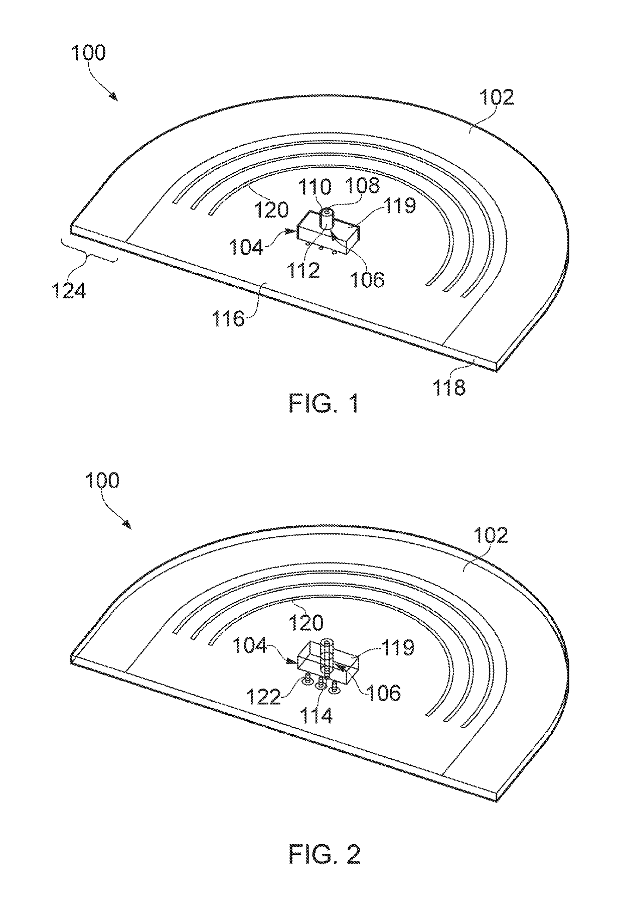
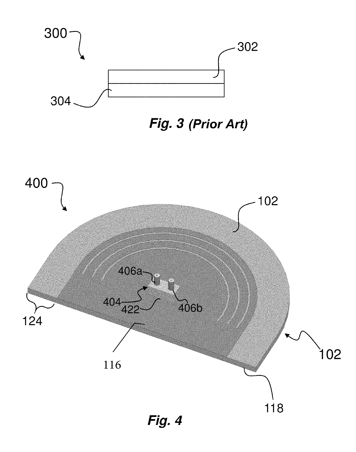
[0013]FIGS. 1 and 2 show a surface wave launcher 100 in accordance with an embodiment of the present invention. The surface wave launcher 100 includes a waveguide section 102 and a feed section 104. The feed section 104 comprises a coaxial cable 106. The coaxial cable 106 includes an inner conductor 108, an insulating layer 110 and an outer conductor 112, as shown in FIG. 1. The feed section 104 also includes a feed pin 114 (FIG. 2) which is connected to the inner conductor 108 at the end of the coaxial cable 106 and couples the inner conductor 108 to the waveguide 102.

[0014]The waveguide 102 comprises a planar conductor 116 as shown in FIG. 1, which forms an upper surface of the waveguide 102. The waveguide 102 preferably also comprises a dielectric layer 118 (FIG. 1), positioned below the planar conductor 116. The dielectric making up the dielectric layer 118 is preferably low loss for the wavelength of operation, i.e. the wavelength of surface waves to be launched. The launcher 1...


PUM


Abstract

A surface wave launcher for launching electromagnetic surface waves, the launcher comprising: a waveguide comprising a planar conductive layer; a feed structure comprising a first conductor, the first conductor coupled to the waveguide at a coupling; wherein the waveguide is arranged to be positioned adjacent to a surface suitable for guiding electromagnetic surface waves; and wherein the planar conductive layer comprises one or more slots each having a pair of longitudinal edge, the one or more slots extending through the conductive layer and arranged such that an axis radially extending from the coupling intersects each pair of longitudinal edges of the one or more slots.

Description

FIELD OF THE INVENTION[0001]This invention relates to surface wave launchers.BACKGROUND TO THE INVENTION[0002]The applicant's prior published patent application GB2494435A discloses a communication system which utilises a guiding medium which is suitable for sustaining electromagnetic surface waves. The applicant's prior published application GB2516764A presents various applications and improvements to the system disclosed in GB2494435A. The contents of GB2494435A and GB2516764A are hereby incorporated by reference. The present application presents various additional improvements to the systems discloses in GB2494435A and GB2516764A.[0003]Surface wave launchers exist that are highly efficient at propagating surface waves onto the surface of a guiding medium. Such propagation efficiency is, however, often achieved to the detriment of device compactness; highly efficient devices are often thick and cumbersome and complex to construct. Surface wave launchers having a very small footpri...

Claims


Application Information

Patent Timeline
Patent Type & Authority Patents(United States)
IPC IPC(8): H01P3/10H01Q13/20H01P5/08H01P3/12H01Q13/00
CPCH01P3/10H01P3/122H01P5/087H01Q13/203H01Q13/00H01P5/08H01P3/00
Inventor JESSUP, MICHAEL
Owner ROKE MANOR RES LTD
Why Eureka
Try Eureka