
LNOI suspended spot size converter and process implementation method thereof

A mode spot converter and process technology, applied in the field of integrated photonics, can solve the problems of high structural requirements, limited optical mode size amplification capability, unfavorable device packaging application, etc., and achieve the effect of reducing end-face reflection and increasing mechanical strength

Active Publication Date: 2020-09-15
NO 55 INST CHINA ELECTRONIC SCI & TECHNOLOGYGROUP CO LTD
View PDF11 Cites 11 Cited by
  • Summary
  • Abstract
  • Description
  • Claims
  • Application Information

AI Technical Summary

Problems solved by technology

[0005] However, the grating coupling scheme in (1) is easily affected by factors such as wavelength and polarization, which is not conducive to device packaging applications; the scheme (2) has limited ability to amplify the size of the optical mode, especially in the vertical direction, and usually requires a tapered The low-loss coupling effect between the optical fiber and the LNOI optical waveguide can only be achieved after the lens fiber reduces the size of the optical mode in the optical fiber. This coupling method has relatively high structural requirements for the coupling optical fiber and the LNOI optical waveguide mode-spot converter.

Method used


Image

  • LNOI suspended spot size converter and process implementation method thereof
  • LNOI suspended spot size converter and process implementation method thereof
  • LNOI suspended spot size converter and process implementation method thereof

Examples


Embodiment 2

[0049] Such as Figure 4 As shown, the LNOI optical waveguide core layer 7 is a rectangular optical waveguide structure 7-2.

[0050] Such as Figure 5 As shown, a process realization method of LNOI floating mode spot converter includes the following steps:

[0051] Step 1) On the surface layer of the LNOI material, a hard mask is prepared by spin-coating photoresist, exposure, development, metal evaporation, and wet stripping; and under the protection of the hard mask, through a dry etching process, The LNOI optical waveguide core layer 7 is etched;

[0052] Step 2) Etching of LNOI tapered core layer 5 and transition structure 6;

[0053] On the surface layer of the LNOI optical waveguide core layer 7, a hard mask is prepared by spin-coating photoresist, exposure, development, metal evaporation, and wet stripping; and under the protection of the hard mask, through a dry etching process, Etch the LNOI tapered core layer 5 and transition structure 6 to SiO 2 Lower cladding 8-2;

[0054...


PUM


Abstract

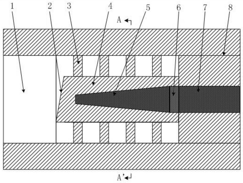
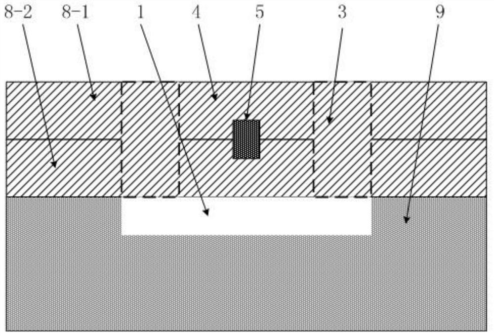
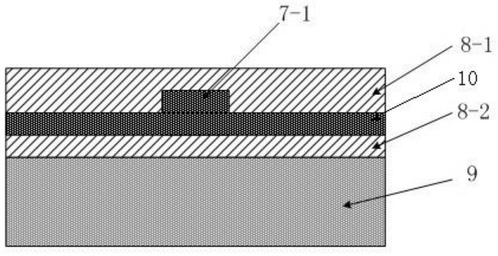
The invention discloses an LNOI (Lithium Niobate on Insulator) suspended spot size converter and a process implementation method thereof. The LNOI suspended spot size converter comprises an optical fiber fixing groove, an optical coupling end face, a SiO2 cantilever beam supporting structure, a SiO2 suspended optical waveguide, an LNOI conical core layer, a transition structure, an LNOI optical waveguide core layer, a SiO2 cladding and a chip substrate. The LNOI conical core layer is embedded in the middle of the SiO2 suspended optical waveguide, and the LNOI optical waveguide core layer is located in a space defined by the transition structure and the SiO2 cladding; the SiO2 suspended optical waveguide, the transition structure and the SiO2 cladding are connected in sequence, and the embedded LNOI conical core layer is in accurate butt joint with the LNOI optical waveguide core layer. According to the converter, transverse and longitudinal simultaneous conversion of the optical mode size in the LNOI optical waveguide is achieved, the requirement for matching a submicron LNOI optical waveguide with the optical fiber mode size can be met, and the mode converter is suitable for botha ridge-shaped LNOI optical waveguide and a rectangular LNOI optical waveguide.

Description

Technical field [0001] The invention relates to the field of integrated photonics, and relates to an LNOI floating mode spot converter and a process realization method thereof. Background technique [0002] Thin film lithium niobate (LNOI, Lithium Niobate on Insulator) material is a new type of integrated optoelectronic chip material, not only has LiNbO 3 The bulk material itself has superior performance, and after being thinned, it has stronger light confinement ability, higher integration and higher electro-optical control efficiency than traditional bulk materials. Especially, Si-based LNOI material is thin film LiNbO 3 The photonic technology and the optoelectronic monolithic integration of Si-CMOS circuits provide an excellent platform and have broad application prospects in the field of optoelectronic integration. [0003] For the LNOI photonic chip, insertion loss is one of the key factors that determine whether it meets the actual application requirements. The factors affe...

Claims


Application Information

Patent Timeline
Patent Type & Authority Applications(China)
IPC IPC(8): G02B6/122G02B6/136G02B6/14
CPCG02B6/1228G02B6/14G02B6/136
Inventor 钱广周奉杰唐杰顾晓文孔月婵陈堂胜
Owner NO 55 INST CHINA ELECTRONIC SCI & TECHNOLOGYGROUP CO LTD
Learn More